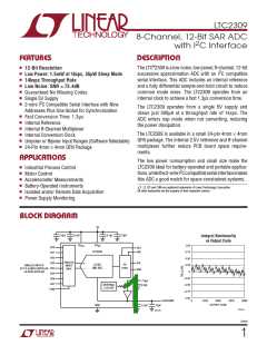
LTC2309
I2C TIMING CHARACTERISTICS The
l
denotes the specifications which apply over the full operating
temperature range, otherwise specifications are at T = 25°C. (Note 4)
A
SYMBOL PARAMETER
CONDITIONS
MIN
TYP
MAX
UNITS
kHz
μs
l
l
l
l
l
l
l
l
l
l
l
f
t
t
t
t
t
t
t
t
t
t
SCL Clock Frequency
400
SCL
Hold Time (Repeated) Start Condition
Low Period of the SCL Pin
0.6
1.3
HD(SDA)
LOW
μs
High Period of the SCL Pin
0.6
μs
HIGH
SU(STA)
HD(DAT)
SU(DAT)
r
Set-Up Time for a Repeated Start Condition
Data Hold Time
0.6
μs
0
0.9
μs
Data Set-Up Time
100
ns
Rise Time for SDA/SCL Signals
Fall Time for SDA/SCL Signals
Set-Up Time for Stop Condition
Bus Free Time Between a Stop and Start Condition
(Note 12)
(Note 12)
20 + 0.1C
20 + 0.1C
0.6
300
300
ns
B
ns
f
B
μs
SU(STO)
BUF
1.3
μs
ADC TIMING CHARACTERISTICS The
l
denotes the specifications which apply over the full operating
temperature range, otherwise specifications are at T = 25°C. (Note 4)
A
SYMBOL PARAMETER
CONDITIONS
MIN
TYP
1.3
MAX
14
UNITS
ksps
μs
l
l
l
f
t
t
t
Throughput Rate (Successive Reads)
Conversion Time
SMPL
CONV
(Note 9)
(Note 9)
1.8
Acquisition Time
240
ns
ACQ
REFCOMP Wake-Up Time (Note 13)
C
= 10μF, C = 2.2μF
200
ms
REFWAKE
REFCOMP
REF
Note 7: Bipolar zero error is the offset voltage measured from –0.5LSB
when the output code flickers between 0000 0000 0000 and 1111 1111
1111. Unipolar zero error is the offset voltage measured from +0.5LSB
when the output code flickers between 0000 0000 0000 and 0000 0000
0001.
Note 1: Stresses beyond those listed under Absolute Maximum Ratings
may cause permanent damage to the device. Exposure to any Absolute
Maximum Rating condition for extended periods may affect device
reliability and lifetime.
Note 2: All voltage values are with respect to ground with AV and DV
DD
DD
Note 8: Full-scale bipolar error is the worst-case of –FS or +FS untrimmed
deviation from ideal first and last code transitions and includes the effect
of offset error. Unipolar full-scale error is the deviation of the last code
transition from ideal and includes the effect of offset error.
wired together (unless otherwise noted).
Note 3: When these pin voltages are taken below ground or above V
they will be clamped by internal diodes. These products can handle input
currents greater than 100mA below ground or above V without latchup.
,
DD
DD
Note 9: Guaranteed by design, not subject to test.
Note 4: AV = 5V, DV = 5V, f = 14ksps internal reference unless
DD
DD
SMPL
Note 10: All specifications in dB are referred to a full-scale 2.048V input
otherwise noted.
with a 2.5V reference voltage.
Note 5: Linearity, offset and full-scale specifications apply for a
Note 11: Full linear bandwidth is defined as the full-scale input frequency
single-ended analog input with respect to COM.
at which the SINAD degrades to 60dB or 10 bits of accuracy.
Note 6: Integral nonlinearity is defined as the deviation of a code from a
straight line passing through the actual endpoints of the transfer curve.
The deviation is measured from the center of the quantization band.
Note 12: C = capacitance of one bus line in pF (10pF ≤ C ≤ 400pF).
B
B
Note 13: REFCOMP wake-up time is the time required for the REFCOMP
pin to settle within 0.5LSB at 12-bit resolution of its final value after
waking up from SLEEP mode.
2309f
5

 Linear [ Linear ]