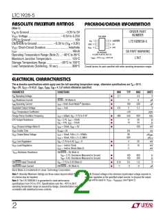
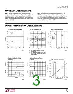
LTC1928-5
U
W U U
APPLICATIONS INFORMATION
Power-On Reset
General Layout Considerations
Upon initial power-up, a power-on reset circuit ensures
that the internal functions are correctly initialized. Once
VIN reaches about 1V, the power-on reset circuit will
enable the part as long as the CN/SHDN pin is not pulled
low.
Due to the high switching frequency and high transient
currents produced by the device, careful board layout is a
must. A clean board layout using a ground plane and short
connections to all capacitors will improve noise perfor-
mance and ensure proper regulation.
Thermal Considerations
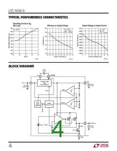
Measuring Output Noise
The power handling capability of the device will be limited
by the maximum rated junction temperature (125°C). The
devicedissipationPD =IOUT(2VIN –VOUT)+VIN(2mA). The
device dissipates the majority of its heat through its pins,
especially GND (Pin 2). Thermal resistance to ambient can
be optimized by connecting GND to a large copper region
on the PCB, which serves as a heat sink. Applications that
operatetheLTC1928-5nearmaximumpowerlevelsshould
maximize the copper area at all pins except CP and
CN/SHDN and ensure that there is some airflow over the
part to carry away excess heat.
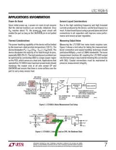
Measuring the LTC1928 low noise levels requires care.
Figure 3 shows a test setup for taking the measurement.
Good connection and signal handling technique should
yield about 800µVP-P over a 2.5MHz bandwidth. The noise
measurement involves AC coupling the LTC1928 output
into the test setup’s input and terminating this connection
with 50Ω. Coaxial connections must be maintained to
preserve measurement integrity.
BNC CABLES
OR COUPLERS
COUPLING
CAPACITOR
LTC1928
PREAMP
1822
BATTERY OR
LOW NOISE DC
POWER SUPPLY
V
OUT
+
–
DEMO
INPUT
BANDWIDTH
FILTER
BOARD
10×
OSCILLOSCOPE
R*
R
LOAD
R*
CONNECT BNC AND
GROUND TO THE
OUTPUT CAPACITOR
GROUND TERMINAL
R
PLACE BANDWIDTH FILTER
COMPONENTS IN SHIELDED BOX
WITH COAXIAL CONNECTORS
LOAD
R*
PLACE COUPLING
CAPACITOR IN SHIELDED
BOX WITH COAXIAL
CONNECTOR
*50Ω TERMINATIONS NOTE: KEEP BNC CONNECTIONS
19285 F03
HP-11048C OR
EQUIVALENT
AS SHORT AS POSSIBLE
Figure 3. LTC1928-5 Noise Measurement Test Setup
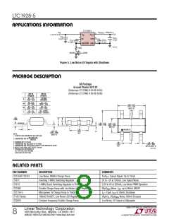
LTC1928-5
V
< 800µV
P-P
RIPPLE
ADDITIONAL
LDO
3
2
1
4
5
6
CPO
CP
V
5V
OUT
C
OUT
C
CPO
IN
4.7µF
4.7µF
GND
C
FLY
OUT
3.3V
10µF
0.47µF
V
IN
CN/SHDN
V
IN
GND
3V
C
IN
4.7µF
19285 F04
Figure 4. LTC1928-5, External Load on CPO, No Shutdown State
Information furnished by Linear Technology Corporation is believed to be accurate and reliable.
However, no responsibility is assumed for its use. Linear Technology Corporation makes no represen-
tationthattheinterconnectionofitscircuitsasdescribedhereinwillnotinfringeonexistingpatentrights.
7

 Linear [ Linear ]