LTC1928-5
U
U
U
PIN FUNCTIONS
VIN (Pin 1): Input Voltage, 2.7V to 4.4V. VIN should be
bypassed with a ≥2µF low ESR capacitor as close to the
pin as possible for best performance. A minimum capaci-
tance value of 0.1µF is required.
CPO (Pin 4): Boosted Unregulated Voltage. Approxi-
mately 1.95VIN at low loads. Bypass with a ≥2µF low ESR
capacitor.
CP (Pin 5): Flying Capacitor Positive Input.
GND (Pin 2): System Ground.
CN/SHDN (Pin 6): Flying Capacitor Negative Input and
SHDN. When this pin is pulled to ground through a 100Ω
resistor, the part will go into shutdown within approxi-
mately 30µs.
V
OUT (Pin 3): Low Noise Regulated Output Voltage. VOUT
should be bypassed with a ≥2µF low ESR capacitor as
closetothepinaspossibleforbestperformance.TheVOUT
voltage is internally set to 5V.
U
W U U
APPLICATIONS INFORMATION
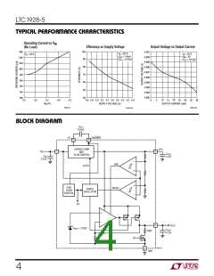
Operation
The LDO is used to filter the ripple on CPO and to set an
output voltage independent of CPO. VOUT is set by an
internal reference and resistor divider. The LDO requires a
capacitoronVOUT forstabilityandimprovedloadtransient
response. A low ESR capacitor of ≥2µF should be used.
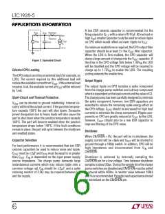
The LTC1928-5 uses a switched-capacitor charge pump
to generate a CPO voltage of approximately 2VIN. CPO
powers an internal low dropout linear regulator that sup-
plies a regulated output at VOUT. Internal comparators are
used to sense CPO and VIN voltages for power-up condi-
tioning. The output current is sensed to determine the
chargepumpoperatingmode.Atrimmedinternalbandgap
is used as the voltage reference and a trimmed internal
oscillator is used to control the charge pump switches.
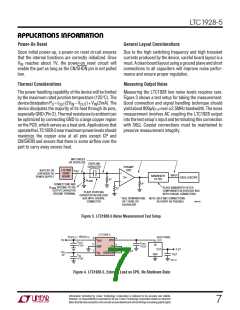
Maximum IOUT Calculations
The maximum available current can be calculated based
on the open circuit CPO voltage, the dropout voltage of the
LDO and the effective output resistance of the charge
pump. The open circuit CPO voltage is approximately 2VIN
(see Figure 2).
The charge pump is a doubler configuration that uses one
external flying capacitor. When enabled, a 2-phase
nonoverlappingclockcontrolsthechargepumpswitches.
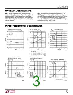
At start-up, the LDO is disabled and the load is removed
fromCPO. WhenCPOreaches1.75VIN theLDOisenabled.
If CPO falls below 1.45VIN the LDO will be disabled. Gen-
erally, the charge pump runs open loop with continuous
clocking for low noise. If CPO is greater than 1.95VIN and
IOUT is less than 200µA, the charge pump will operate in
Burst Mode operation for increased efficiency but slightly
higher output noise. In Burst Mode operation, the clock is
disabled when CPO reaches 1.95VIN and enabled when
CPO droops by about 150mV. The switching frequency is
precisely controlled to ensure that the frequency is above
455kHz and at the optimum rate to ensure maximum effi-
ciency. The switch edge rates are also controlled to mini-
mize noise. The effective output resistance at CPO is
dependent on the voltage at VIN, CPO, the flying capacitor
value CFLY and the junction temperature. A low ESR ca-
pacitorof≥2µFshouldbeusedatCPOforminimumnoise.
Example:
VIN = 3V
VOUT = 5V
RCPO = 30Ω
Maximum unloaded CPO voltage = 2VIN = 6V
VDROPOUT(MAX) = 100mV
IOUT(MAX) = (2VIN – VDROPOUT(MAX) – VOUT)/RCPO
= (6V – 0.1V – 5V)/30Ω = 30mA
VCPO must be greater than 1.45VIN = 4.35V. To confirm
this, calculate VCPO
:
VCPO = 6V – (30mA • 30Ω) = 5.1V
For minimum noise applications the LDO must be kept out
of dropout to prevent CPO noise from coupling into VOUT
.
5

 Linear [ Linear ]