LTC1928-5
ELECTRICAL CHARACTERISTICS
Note 4: Operating conditions are limited by maximum junction
temperature. The regulated output specification will not apply for all
possible combinations of input voltage and output current. When
operating at maximum input voltage, the output current range may be
limited. When operating at maximum output current, the input voltage
range may be limited.
Note 5: CN/SHDN must be driven with a source impedance of at least
100Ω (R ) to prevent damage to the part. This pin is multiplexed
SOURCE
and may be connected through a low switch impedance to V . There may
IN
be a large amount of current (V /R
) until the shutdown state
IN SOURCE
occurs after which the charge pump switches at CN/SHDN become high
impedance and the current will fall to <8µA.
U W
TYPICAL PERFOR A CE CHARACTERISTICS
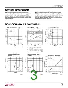
CPO Output Resistance vs VIN
Min and Max VCPO vs VIN
VOUT Transient Response
9
8
7
6
5
4
3
35
30
25
20
15
10
5
10
5
T
C
I
= 25°C
T = 25°C
A
A
= 0.47µF
FLY
= 10mA
OUT
V
= 2(V )
IN
CPO
0
T
= 25°C
A
(A)
V
V
C
= 3V
–5
–10
15
10
5
IN
= 5V
OUT
OUT
(B)
= 4.7µF
V
= 1.45(V )
IN
CPO
0
2.5
3.0
3.5
(V)
4.0
4.5
250
2.5
3.0
3.5
(V)
4.0
4.5
0
50
100
150
TIME (µs)
200
300
V
V
IN
IN
19285 G01
19285 G03
(A) THE MAXIMUM GENERATED NO LOAD
CPO VOLTAGE
(B) THE MINIMUM ALLOWABLE CPO VOLTAGE,
AT FULL LOAD, TO ENSURE THAT THE LDO
IS NOT DISABLED
19285 G02
Shutdown to Enable Timing
(Figure 5)
Enable to Shutdown Timing
(Figure 5)
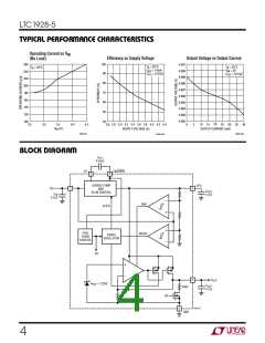
VOUT Voltage vs Temperature
5.040
5.030
5.020
5.010
5.000
4.990
4.980
V
OUT
= 3V
IN
2
2
0
5
4
3
2
1
0
I
= 10mA
0
5
4
3
2
1
0
NO LOAD
T
= 25°C
A
T
= 25°C
V
V
I
= 3V
A
IN
OUT
V
V
C
= 3V
= 5V
IN
OUT
OUT
= 5V
= 10mA
OUT
= 4.7µF
C
= C
= 4.7µF
OUT
CPO
50
TEMPERATURE (°C)
100 125
–50 –25
0
25
75
200µs/DIV
1ms/DIV
19285 G04
19285 G05
19285 G06
3

 Linear [ Linear ]