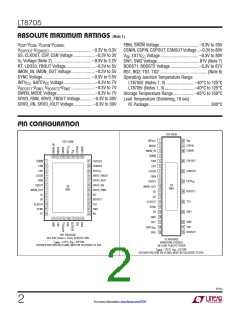
LT8705
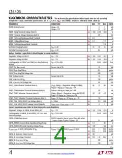
ELECTRICAL CHARACTERISTICS The l denotes the specifications which apply over the full operating
temperature range, otherwise specifications are at TA = 25°C. VIN = 12V, SHDN = 3V unless otherwise noted. (Note 3)
PARAMETER
CONDITIONS
MIN
TYP
MAX UNITS
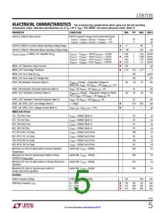
l
l
SYNC High Level for Synchronization
SYNC Low Level for Synchronization
SYNC Clock Pulse Duty Cycle
Recommended Minimum SYNC Ratio f
CLKOUT Output Voltage High
CLKOUT Output Voltage Low
CLKOUT Duty Cycle
1.3
V
0.5
80
V
V
= 0V to 2V
20
%
SYNC
/f
3/4
2.45
25
SYNC OSC
1mA Out of CLKOUT Pin
1mA Into CLKOUT Pin
2.3
2.55
100
V
mV
T = –40°C
21.4
42.5
75
%
%
%
J
T = 25°C
J
T = 125°C
J
CLKOUT Rise Time
CLKOUT Fall Time
CLKOUT Phase Delay
C
C
= 200pF
= 200pF
30
25
ns
ns
LOAD
LOAD
l
SYNC Rising to CLKOUT Rising, f
= 100kHz
160
180
200
Deg
OSC
Note 1: Stresses beyond those listed under Absolute Maximum Ratings
may cause permanent damage to the device. Exposure to any Absolute
Maximum Rating condition for extended periods may affect device
reliability and lifetime.
Note 4: Rise and fall times are measured using 10% and 90% levels. Delay
times are measured using 50% levels.
Note 5: This specification not applicable in the FE38 package.
Note 6: Do not apply a voltage or current source to these pins. They must
be connected to capacitive loads only, otherwise permanent damage may
occur.
Note 7: Negative voltages on the SW1 and SW2 pins are limited, in an
application, by the body diodes of the external NMOS devices, M2 and
M3, or parallel Schottky diodes when present. The SW1 and SW2 pins
are tolerant of these negative voltages in excess of one diode drop below
ground, guaranteed by design.
Note 2: Do not force voltage on the V pin.
C
Note 3: The LT8705E is guaranteed to meet performance specifications
from 0°C to 125°C junction temperature. Specifications over the –40°C
to 125°C operating junction temperature range are assured by design,
characterization and correlation with statistical process controls. The
LT8705I is guaranteed over the full –40°C to 125°C junction temperature
range.
8705p
6
For more information www.linear.com/8705

 Linear [ Linear ]