LT8705
ELECTRICAL CHARACTERISTICS The l denotes the specifications which apply over the full operating
temperature range, otherwise specifications are at TA = 25°C. VIN = 12V, SHDN = 3V unless otherwise noted. (Note 3)
PARAMETER
CONDITIONS
MIN
TYP
MAX UNITS
SHDN Pin Bias Current
V
SHDN
V
SHDN
= 3V
= 12V
0
11
1
22
µA
µA
l
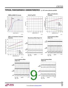
SWEN Rising Threshold Voltage (Note 5)
SWEN Threshold Voltage Hysteresis (Note 5)
MODE Pin Forced Continuous Mode Threshold
MODE Pin Burst Mode Range
1.156 1.206 1.256
V
mV
V
22
l
l
l
0.4
1.0
1.7
2.3
25
V
MODE Pin Discontinuous Mode Threshold
Soft-Start Charging Current
V
V
V
= 0.5V
13
19
µA
µA
SS
Soft-Start Discharge Current
= 0.5V
9.5
SS
Voltage Regulator Loops (Refer to Block Diagram to Locate Amplifiers)
l
l
Regulation Voltage for FBOUT
Regulation Voltage for FBIN
V = 1.2V
1.193 1.207 1.217
1.187 1.205 1.220
0.002 0.005
V
V
C
V = 1.2V
C
Line Regulation for FBOUT and FBIN Error Amp Reference
Voltage
V
= 12V to 80V
%/V
IN
FBOUT Pin Bias Current
Current Out of Pin
Current Out of Pin
15
315
220
10
nA
µmho
V/V
FBOUT Error Amp EA4 g
m
FBOUT Error Amp EA4 Voltage Gain
FBIN Pin Bias Current
nA
FBIN Error Amp EA3 g
130
90
µmho
V/V
m
FBIN Error Amp EA3 Voltage Gain
SRVO_FBIN Activation Threshold (Note 5)
(V
FBOUT
Falling) – (Regulation Voltage for FBIN),
56
72
89
mV
FBIN
V
= V
= V
= 0V
IMON_IN
IMON_OUT
SRVO_FBIN Activation Threshold Hysteresis (Note 5)
SRVO_FBOUT Activation Threshold (Note 5)
V
= V
= V
= 0V
33
mV
mV
FBOUT
IMON_IN
IMON_OUT
(V
V
Rising) – (Regulation Voltage for FBOUT),
–37
–29
–21
FBOUT
= 3V, V
= V
= 0V
FBIN
IMON_IN
IMON_OUT
SRVO_FBOUT Activation Threshold Hysteresis (Note 5)
SRVO_FBIN, SRVO_FBOUT Low Voltage (Note 5)
SRVO_FBIN, SRVO_FBOUT Leakage Current (Note 5)
V
= 3V, V
= 0V, V
= 0V
15
110
0
mV
mV
µA
FBIN
IMON_IN
IMON_OUT
l
l
I = 100μA
330
1
V
= V
= 2.5V
SRVO_FBOUT
SRVO_FBIN
Current Regulation Loops (Refer to Block Diagram to Locate Amplifiers)
l
Regulation Voltages for IMON_IN and IMON_OUT
V = 1.2V
1.191 1.208 1.223
0.002 0.005
V
C
Line Regulation for IMON_IN and IMON_OUT Error Amp
Reference Voltage
V
= 12V to 80V
%/V
IN
CSPIN, CSNIN Bias Current
BOOST Capacitor Charge Control Block Not Active
I
+ I
, V
= V = 12V
CSNIN
31
µA
V
CSPIN
CSNIN CSPIN
l
l
CSPIN, CSNIN Common Mode Operating Voltage Range
CSPIN, CSNIN Differential Operating Voltage Range
1.5
80
–100
100
mV
V
to IMON_IN Amplifier A7 g
V
CSPIN
– V
= 50mV, V = 5.025V
CSPIN
0.95
0.94
1
1
1.05
1.06
mmho
mmho
CSPIN-CSNIN
m
CSNIN
l
l
l
IMON_IN Maximum Output Current
IMON_IN Overvoltage Threshold
100
µA
V
1.55
1.61
185
130
1.67
IMON_IN Error Amp EA2 g
µmho
V/V
m
IMON_IN Error Amp EA2 Voltage Gain
8705p
4
For more information www.linear.com/8705

 Linear [ Linear ]