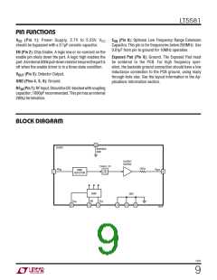
LT5581
The l denotes the specifications which apply over the full operating temperature
ELECTRICAL CHARACTERISTICS
range, otherwise specifications are at TA = 25°C, VCC = 3.3V, EN = 3.3V, unless otherwise noted (Note 2). Test circuit is shown in Figure 1.
PARAMETER
CONDITIONS
Normalized to Output at 25°C, –40°C < T < 85°Cꢁ
MIN
TYP
MAX
UNITS
Output Variation vs Temperature
0.5
dB
A
P
= –27 to –10dBm
IN
Deviation from CW Response
IN
WiMAX OFDMA Preamble
WiMAX OFDM Burst
0.1
0.5
dB
dB
P
= –34 to –4dBm
f
= 5800MHz
RF
RF Input Power Range
Externally Matched to 50ꢀ Source
1dB Linearity Error
–25 to 6
dBm
dB
Linear Dynamic Range, CW (Note 3)
Output Slope
31
31
–33
1
mV/dB
dBm
dB
Logarithmic Intercept (Note 5)
Output Variation vs Temperature
Normalized to Output at 25°C, –40°C < T < 85°Cꢁ
A
P
= –25 to +6dBm
IN
Output Variation vs Temperature
Normalized to Output at 25°C, –40°C < T < 85°Cꢁ
IN
0.5
0.2
dB
dB
A
P
= –20 to +6dBm
Deviation from CW Response
Output
WiMAX OFDM Burstꢁ P = –25 to 6dBm
IN
Output DC Voltage
No Signal Applied to RF Input
180
300
5/5
1
mV
ꢀ
Output Impedance
Internal Series Resistor Allows for Off-Chip Filter Cap
Output Current Sourcing/Sinking
Rise Time
mA
μs
0.2V to 1.6V, 10% to 90%, f = 2140MHz
RF
Fall Time
1.6V to 0.2V, 10% to 90%, f = 2140MHz
8
μs
RF
Power Supply Rejection Ratio (Note 6)
Integrated Output Voltage Noise
Enable (EN) Low = Off, High = On
EN Input High Voltage (On)
EN Input Low Voltage (Off)
Enable Pin Input Current
Turn-On Timeꢁ CW RF input
Settling Timeꢁ RF Pulse
Power Supply
For Over Operating Input Power Range
49
dB
1kHz to 6.5kHz Integration BW, P = 0dBm CW
150
μV
RMS
IN
l
l
2
V
V
0.3
EN = 3.3V
20
1
μA
μs
μs
V
Within 10% of Final Valueꢁ P = 0dBm
IN
OUT
OUT
V
Within 10% of Final Valueꢁ P = 0dBm
1
IN
l
Supply Voltage
2.7
3.3
1.4
0.2
5.25
6
V
mA
μA
Supply Current
No RF Input Signal
EN = 0.3V, V = 3.3V
Shutdown Current
CC
Note 1: Stresses beyond those listed under Absolute Maximum Ratings
may cause permanent damage to the device. Exposure to any Absolute
Maximum Rating condition for extended periods may affect device
reliability and lifetime.
Note 4: An external capacitor at the C pin should be used for input
frequencies below 250MHz. Lower frequency operation results in
excessive RF ripple in the output voltage.
SQ
Note 5: Logarithmic intercept is an extrapolated input power level from the
Note 2: The LT5581 is guaranteed to meet specified performance from
best fitted log-linear straight line, where the output voltage is 0V.
–40°C to 85°C.
Note 6: PSRR is determined as the dB value of the change in V
voltage
OUT
Note 3: The linearity error is calculated by the difference between the
incremental slope of the output and the average output slope from
–20dBm to 0dBm. The dynamic range is defined as the range over which
the linearity error is within 1dB.
over the change in V supply voltage.
Note 7: Not production tested. Guaranteed by design and correlation to
production tested parameters.
CC
5581f
4

 Linear [ Linear ]