LT5581
ABSOLUTE MAXIMUM RATINGS
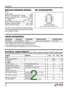
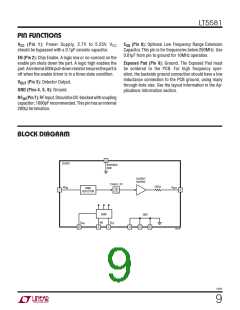
PIN CONFIGURATION
(Note 1)
Supply Voltage.........................................................5.5V
Maximum Input Signal Power—Average.............15dBm
Maximum Input Signal Power—Peak (Note 7) ....25dBm
TOP VIEW
V
1
2
3
4
8
7
6
5
C
SQ
CC
EN
RF
IN
DC Voltage at RF ....................................... –0.3V to 2V
9
IN
V
GND
GND
OUT
V
Voltage....................................–0.3V to V + 0.3V
OUT
CC
GND
Maximum Junction Temperature, T
............... 150°C
JMAX
Operating Temperature Range.................. –40°C to 85°C
DDB PACKAGE
8-LEAD (3mm s 2mm) PLASTIC DFN
= 150°C, θ = 76°C/W
Storage Temperature Range................... –65°C to 150°C
T
JMAX
JA
EXPOSED PAD (PIN 9) IS GND, MUST BE SOLDERED TO PCB
CAUTION:Thispartissensitivetoelectrostaticdischarge.It
isveryimportantthatproperESDprecautionsbeobserved
when handling the LT5581.
ORDER INFORMATION
LEAD FREE FINISH
TAPE AND REEL
PART MARKING
PACKAGE DESCRIPTION
8-Lead (3mm × 2mm) Plastic DFN
TEMPERATURE RANGE
–40°C to 85°C
LT5581IDDB#PBF
LT5581IDDB#TRPBF
LDKM
Consult LTC Marketing for parts specified with wider operating temperature ranges.
Consult LTC Marketing for information on non-standard lead based finish parts.
For more information on lead free part marking, go to: http://www.linear.com/leadfree/
For more information on tape and reel specifications, go to: http://www.linear.com/tapeandreel/
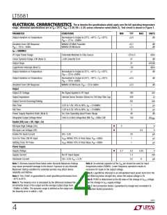
ELECTRICAL CHARACTERISTICS The l denotes the specifications which apply over the full operating temperature
range, otherwise specifications are at TA = 25°C, VCC = 3.3V, EN = 3.3V, unless otherwise noted (Note 2). Test circuit is shown in Figure 1.
PARAMETER
CONDITIONS
MIN
TYP
MAX
UNITS
AC Input
Input Frequency Range (Note 4)
Input Impedance
10-6000
205||1.6
MHz
ꢀ||pF
f
= 450MHz
RF
RF Input Power Range
Externally Matched to 50ꢀ Source
1dB Linearity Error
–34 to 6
40
dBm
dB
Linear Dynamic Range, CW (Note 3)
Linear Dynamic Range, CDMA (Note 3)
Output Slope
1dB Linearity Errorꢁ CDMA 4-Carrier
40
dB
31
mV/dB
dBm
dB
Logarithmic Intercept (Note 5)
Output Variation vs Temperature
–42
1
Normalized to Output at 25˚C, –40°C < T < 85°Cꢁ
A
P
IN
= –34 to +6dBm
Output Variation vs Temperature
Deviation from CW Responseꢁ
Normalized to Output at 25°C, –40°C < T < 85°Cꢁ
IN
0.5
dB
A
P
= –27 to –10dBm
TETRA π/4 DQPSK
CDMA 4-Carrier 64-Channel Fwd 1.23Mcps
0.1
0.5
dB
dB
P
= –34dBm to 0dBm
IN
5581f
2

 Linear [ Linear ]