LT3840
applicaTions inForMaTion
The soft-start capacitor is reset under fault conditions
Switching Frequency Synchronization
including UVLO, EN, OVLO, overtemperature shutdown
The oscillator can be synchronized to an external clock.
and INTV UVLO. The soft-start pin is clamped through
CC
Set the R resistor 15% below the lowest synchronized
T
a diode to the V pin. Therefore, the soft-start pin is reset
FB
frequency. The rising edge of the SYNC pin waveform
triggers the discharge of the internal oscillator capacitor.
If unused, connect the SYNC pin to GND.
duringashort-circuitminimizingovershootuponrecovery.
EN, UVLO and OVLO
EN has a precision voltage threshold with hysteresis to
enable the LT3840 auxiliary bias supply and synchronous
Layout Considerations Checklist
The following is a list of recommended layout consider-
ations:
controller. The pin is typically connected to V through a
IN
resistor divider, however, it can be directly connected to
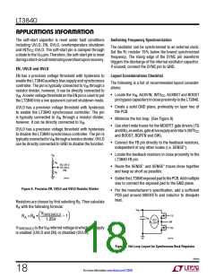
• Locate the V , AUXVIN, INTV , AUXBST and BOOST
V . A lower voltage threshold on the EN pin is used to put
IN
CC
IN
pin bypass capacitors in close proximity to the LT3840.
the LT3840 into a low quiescent current shutdown mode.
• Create a solid GND plane, preferably on layer two of
UVLO has a precision voltage threshold with hysteresis
to enable the LT3840 synchronous controller. The pin
the PCB.
is typically connected to V through a resistor divider,
IN
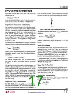
• Minimize the hot loop. (See Figure 9)
however, it can be directly connected to V .
IN
• Use short wide traces for the MOSFET gate drivers (TG
OVLO has a precision voltage threshold with hysteresis
to disable the LT3840 synchronous controller. The pin is
andBG),aswellas,gatedrivesupplyandreturn(INTV
and BOOST, BGRTN and SW).
CC
typicallyconnectedtoV througharesistordivider.OVLO
IN
• Connect the FB pin directly to the feedback resistors,
can be directly connected to GND to disable the function.
+
independent of any other nodes (i.e. SENSE ).
• Locate the feedback resistors in close proximity to the
V
IN
LT3840 FB pin.
R
A
B
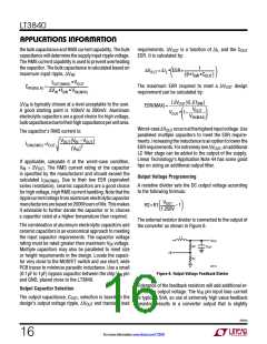
EN, UVLO
OR OVLO
PIN
–
+
• Route the SENSE and SENSE traces close together
and keep as short as possible.
R
3840 F08
• SoldertheLT3840exposedpadtothePCB.Addmultiple
vias to connect the exposed pad to the GND plane.
Figure 8. Precision EN, UVLO and OVLO Resistor Divider
• Per the manufacturer’s specification, add a sufficient
PCB pad around MOSFETs and inductor to dissipate
heat.
Resistors are chosen by first selecting R . Then calculate
B
R with the following formula:
A
V
IN
V
THRESHOLD
1.25V
TG
SW
RA =RB •
– 1
C
IN
HOT
LOOP
BG
V
is the V referred voltage at which the supply
IN
THRESHOLD
is enabled (UVLO and EN) or disabled (OVLO).
3840 F09
Figure 9. Hot Loop Layout for Synchronous Buck Regulator
3840fa
18
For more information www.linear.com/LT3840

 Linear [ Linear ]