LTC3703
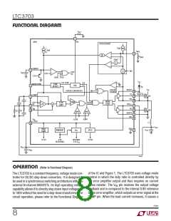
operaTion (Refer to Functional Diagram)
Buck or Boost Mode Operation
operating mode with the following exceptions: in boost
mode, pulse-skip mode operation is always disabled
regardless of the level of the MODE/SYNC pin and the
line feedforward compensation is also disabled. The
overcurrent circuitry continues to monitor the load cur-
rent by looking at the drain voltage of the main (bottom
side) MOSFET. In boost mode, however, the peak MOS-
FET current does not equal the load current but instead
ID = ILOAD/(1 – D). This factor needs to be taken into ac-
count when programming the IMAX voltage.
The LTC3703 has the capability of operating both as a
step-down(buck)andstep-up(boost)controller.Inboost
mode, output voltages as high as 80V can be tightly regu-
lated. With the INV pin grounded, the LTC3703 operates
in buck mode with TG driving the main (topside) switch
and BG driving the synchronous (bottom side) switch.
If the INV pin is pulled above 2V, the LTC3703 operates
in boost mode with BG driving the main (bottom side)
switch and TG driving the synchronous (topside) switch.
Internal circuit operation is very similar regardless of the
applicaTions inForMaTion
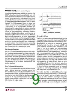
ThebasicLTC3703applicationcircuitisshowninFigure 1.
External component selection is determined by the input
voltageandloadrequirementsasexplainedinthefollowing
operatingfrequencyisthatinnoise-sensitivecommunica-
tions systems, it is often desirable to keep the switching
noise out of a sensitive frequency band.
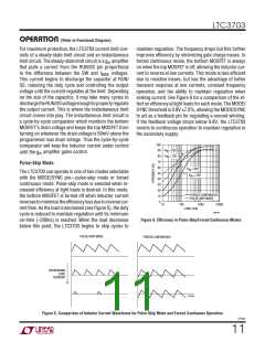
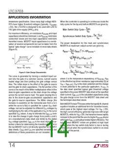
sections. After the operating frequency is selected, R
SET
The LTC3703 uses a constant frequency architecture that
can be programmed over a 100kHz to 600kHz range with
and L can be chosen. The operating frequency and the
inductor are chosen for a desired amount of ripple current
and also to optimize efficiency and component size. Next,
thepowerMOSFETsandD1areselectedbasedonvoltage,
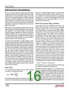
a single resistor from the f
pin to ground, as shown
SET
in Figure 1. The nominal voltage on the f
pin is 1.2V,
SET
and the current that flows from this pin is used to charge
and discharge an internal oscillator capacitor. The value
load and efficiency requirements. C is selected for its
IN
ability to handle the large RMS currents in the converter
of R
for a given operating frequency can be chosen
SET
and C
is chosen with low enough ESR to meet the
OUT
from Figure 7 or from the following equation:
output voltage ripple and transient specifications. Finally,
the loop compensation components are chosen to meet
the desired transient specifications.
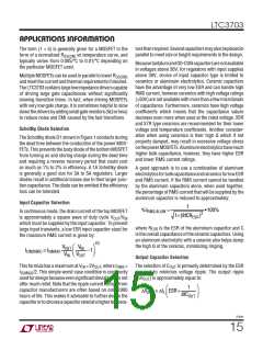
7100
RSET(kΩ)=
f(kHz)–25
1000
Operating Frequency
The choice of operating frequency and inductor value is
a trade-off between efficiency and component size. Low
frequencyoperationimprovesefficiencybyreducingMOS-
FET switching losses and gate charge losses. However,
lower frequency operation requires more inductance for a
given amount of ripple current, resulting in a larger induc-
tor size and higher cost. If the ripple current is allowed
to increase, larger output capacitors may be required to
maintain the same output ripple. For converters with high
100
10
1
200
400
600
800
1000
0
step-down V to V
ratios, another consideration is
FREQUENCY (kHz)
IN
OUT
3703 F07
the minimum on-time of the LTC3703 (see the Minimum
On-TimeConsiderationssection).Afinalconsiderationfor
Figure 7. Timing Resistor (RSET) Value
3703fc
12

 Linear Systems [ Linear Systems ]