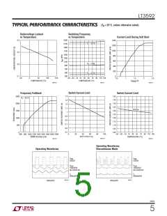
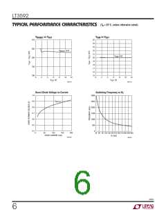
LT3592
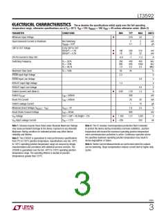
ELECTRICAL CHARACTERISTICS The l denotes the specifications which apply over the full operating
temperature range, otherwise specifications are at TA = 25°C. VIN = 12V, VBOOST = 16V, VOUT = 4V unless otherwise noted. (Note 2)
PARAMETER
CONDITIONS
MIN
TYP
MAX
UNITS
l
Minimum Input Voltage
Input Quiescent Current in Shutdown
3.25
3.6
V
Not Switching
SHDN
2
0.1
3
2
mA
μA
V
= 0.3V
CAP to OUT Voltage
0.4ꢀ CAP to OUT
BRIGHT = 1.4V
BRIGHT = 0.3V
l
l
190
18
200
20
210
22
mV
mV
DA Pin Current to Stop OSC
Switching Frequency
–0.8
–1
–1.2
A
R = 357k
350
800
1.9
400
900
2.2
450
1000
2.5
kHz
kHz
MHz
T
R = 140k
T
R = 48.7k
T
Maximum Duty Cycle
R = 140k
90
94
%
V
T
SHDN Input High Voltage
SHDN Input Low Voltage
BRIGHT Input High Voltage
BRIGHT Input Low Voltage
Switch Current Limit (Note 4)
2.3
0.3
V
1.4
V
0.3
1.5
V
l
0.85
1.25
300
20
A
Switch V
I
I
= 500mA
= 500mA
mV
mA
μA
V
CESAT
SW
Boost Pin Current
30
10
SW
Switch Leakage Current
Minimum Boost Voltage (V
1
– V )
V = 4V
OUT
1.8
800
1.21
2.5
BOOST
IN
Boost Diode Forward Voltage
I
= 50mA
mV
V
DIO
l
l
V
Voltage
OUT = CAP = 4V, Bright = 12V
= 1.21V
1.185
–250
1.235
250
FB
FB
V
Input Leakage Current
V
FB
nA
Note 1: Stresses beyond those listed under Absolute Maximum Ratings
may cause permanent damage to the device. Exposure to any Absolute
Maximum Rating condition for extended periods may affect device
reliability and lifetime.
Note 2: The LT3592E is guaranteed to meet performance specifications
from 0°C to 125°C junction temperature. Specifications over the –40°C
to 125°C operating junction temperature range are assured by design,
characterization and correlation with statistical process controls. The
LT3592I is guaranteed over the full –40°C to 125°C operating junction
temperature range. The operating lifetime is derated at junction
temperatures greater than 125°C.
Note 3: This IC includes overtemperature protection that is intended
to protect the device during momentary overload conditions. Junction
temperature will exceed the maximum operating junction temperature
when overtemperature protection is active. Continuous operation above
the specified maximum operating junction temperature may result in
device degradation or failure.
Note 4: Switch Current Measurements are performed when the outputs
are not switching. Slope compensation reduces current limit at higher duty
cycles.
3592fc
3

 Linear Systems [ Linear Systems ]