LTC4060
W U U
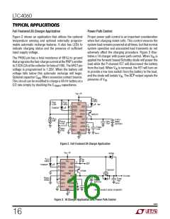
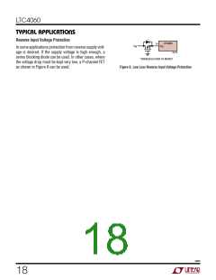
APPLICATIO S I FOR ATIO
U
charging (the DRIVE pin is internally switched to the BAT
pin). Most transistors will meet this requirement as well.
power derating for elevated temperature operation. The
maximum power dissipation of the PNP when charging is:
With low supply voltages, the PNP saturation voltage
(VCESAT) becomes important. The VCESAT must be less
than the minimum supply voltage minus the maximum
voltagedropacrosstheinternalcurrentsenseresistorand
bond wires (approximately 0.08Ω) and maximum battery
voltage presented to the charger accounting for wire I • R
drops.
PD(MAX) (W) = IMAX(VDD(MAX) – VBAT(MIN)
)
V
DD(MAX) is the maximum supply voltage and VBAT(MIN) is
the minimum battery voltage when discharged, but not
less than 0.9V/cell since less than 0.9V/cell invokes
precharge current levels.
Thermal Considerations
V
CESAT (V)<VDD(MIN) –(IBAT(MAX) •0.08Ω+VBAT(MAX))
Internalovertemperatureprotectionisprovidedtoprevent
excessive LTC4060 die temperature during a fault condi-
tion. Iftheinternaldietemperatureexceedsapproximately
145°C, charging stops and the part enters the shutdown
state. The faults can be generated from insuffient heat
sinking, a shorted DRIVE pin or from excessive DRIVE pin
current to the base of an external PNP transistor if it’s in
deepsaturationfromaverylowVCE. Onceintheshutdown
state, charge qualification can be reinitiated only by re-
movingandreplacingthebatteryortogglingtheSHDNpin
low to high or removing and reapplying power to the
charger. This protection is not designed to prevent over-
heating of the PNP pass transistor. Indirectly though, self-
heating of the PNP thermally conducting to the LTC4060
can result in the IC’s junction temperature rising above
145°C, thuscuttingoffthePNP’sbasecurrent. Thisaction
willlimitthePNP’sjunctiontemperaturetosometempera-
ture well above 145°C. The user should insure that the
maximum rated junction temperature is not exceeded
underanynormaloperatingcondition.SeePackage/Order
Information for the θJA of the LTC4060 Exposed Pad
packages. The actual thermal resistance in the application
will vary depending on forced air cooling, use of the
Exposed Pad and other heat sinking means, especially the
amount of copper on the PCB to which the LTC4060 is
attached. The majority of the power dissipated within the
LTC4060 is in the current sense resitor and DRIVE pin
driver as given below:
For example, if it were desired to have a programmed
charge current of 2A with a minimum supply voltage of
4.75V and a maximum battery voltage of 3.6V (2 series
cellsat1.8Veach), thentheminimumoperatingVCESAT is:
VCESAT (V) = 4.75 – (2 • 0.08 + 3.6) = 0.99V
If the PNP transistor cannot achieve the saturation voltage
required, basecurrentwilldramaticallyincrease. Thisisto
be avoided for a number of reasons: DRIVE pin current
may reach current limit resulting in the LTC4060 charac-
teristics going out of specifications, excessive power
dissipation may force the IC into thermal shutdown, or the
battery could discharge because some of the current from
theDRIVEpincouldbepulledfromthebatterythroughthe
forward biased PNP collector base junction.
The actual battery fast charge current (IBAT) is slightly less
than the regulated charge current because the charger
senses the emitter current and the battery charge current
will be reduced by the base current. In terms of β (IC/IB)
IBAT can be calculated as follows:
⎛
⎞
⎟
β
IBAT (A) = 930 •IPROG
⎜
β + 1
⎝
⎠
If β = 100 then IBAT is 1% low. The 1% loss can be easily
compensated for by increasing IPROG by 1%.
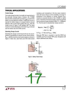
Another important factor to consider when choosing the
PNP pass transistor is its power handling capability. The
transistor’sdatasheetwillusuallygivethemaximumrated
power dissipation at a given ambient temperature with a
PD = (IBAT)2 • 0.08 + IDRIVE (VCC – VEB)
TJ = TA + θJA • PD
VEB is the emitter to base voltage of the external PNP.
4060f
15

 Linear Systems [ Linear Systems ]