LTC4060
W U U
U
APPLICATIO S I FOR ATIO
temperature) at approximately 0°C (5°C – 5°C hysteresis
at VCC = 5V) and then resume when the thermistor falls
below 27k (rising temperature) which will be approxi-
mately 5°C (VNTC = VCLD = 0.86 • VCC typ).
VCC Bypass Capacitor
A 1µF capacitor located close to the LTC4060 will usually
provideadequateinputbypassing.However,cautionmust
be exercised when using multilayer ceramic capacitors.
Because of the self-resonance and high Q characteristics
of some types of ceramic capacitors, along with wiring
inductance, high voltage transients can be generated
undersomeconditionssuchasconnectingordisconnect-
ing a supply input to a hot power source. To reduce the Q
and prevent these transients from exceeding the absolute
maximum voltage rating, consider adding about 1Ω of
resistance in series with the ceramic input capacitor.
Many thermistors with an RCOLD to RHOT ratio of approxi-
mately 7 will work. For lower power dissipation higher
values of thermistor resistance can be used. The Murata
NTH4G series offers resistances of up to 100k at 25°C.
It is important that the thermistor be placed in close
contact with the battery and away from the external PNP
pass transistor to avoid excessive temperature errors on
the sensed battery temperature. Furthermore, since VCC is
a high current path into the LTC4060, it is essential to
minimize voltage drops between the VCC supply pin and
the top of RHOT by Kelvin connecting RHOT directly to the
VCC pin.
BAT Bypass Capacitor
Thisoptionalcapacitor,connectedbetweenBATandGND,
can be used to help filter excessive contact bounce during
the battery monitoring or charging process. The value will
dependuponthecontactbounceopenduration,butistypi-
cally 10µF. Another purpose of this capacitor is to bypass
transient battery load events that might otherwise disrupt
monitoringorcharging.Shouldthebatteryconnectionsnot
be subject to excessive contact bounce or excessive bat-
tery voltage transients, then no BAT pin capacitor is re-
quired. The same caution mentioned above for the VCC by-
pass capacitor applies.
Power Requirements
The DC power input to the VCC pin must always be within
proper limits while charging a battery. Voltages beyond
the absolute maximum ratings may damage the charger
and voltages falling below the UVLO entry thresholds, as
programmed by the SEL0 and SEL1 pins, will likely cause
the charger to enter the shutdown state (when the UVLO
exitthresholdisexceededchargingwillbeginanew).While
the LTC4060 is designed to reject 60Hz or 120Hz supply
ripple,certainprecautionsarerequired.Theinstantaneous
ripple voltage must always be within the above mentioned
limits. Ripple voltage seen across the collector-base junc-
tion of the external PNP pass transistor will slightly modu-
late its beta and hence its base current. Since the emitter
current is precisely regulated by the LTC4060, any modu-
lation of base current will appear at the collector. This
slightly modulated battery charge current into a battery
will usually produce an insignificant modulation voltage at
the battery. However, if excessive wire impedance to the
batteryfromthePNPexists,thenitmaybehelpfultoKelvin
connect the BAT pin to a convenient point closest to the
batterytoreduceripplemagnitudeenteringtheLTC4060’s
battery monitoring circuits. The battery ground imped-
ance should also be managed to limit ripple voltage at the
BAT pin. Excessive ripple into the BAT pin may cause the
charger to deviate from specified performance.
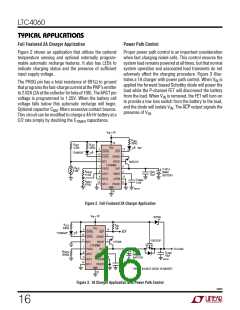
External PNP Transistor
TheexternalPNPpasstransistormusthaveadequatebeta
and breakdown voltages, low saturation voltage and suf-
ficient power dissipation capability that may include heat
sinking.
To provide 2A of charge current with the minimum avail-
able base current drive of 40mA (IDRV min) requires a
minimum PNP beta of 50.
The transistor’s collector to emitter breakdown voltage
must be high enough to withstand the difference between
the maximum supply voltage and minimum battery volt-
age. Almost any transistor will meet this requirement.
Additionally, when no power is supplied to the charger
(VIN=0VandVSENSE=0V),thetransistor’semittertobase
breakdown voltage must be high enough to prevent a
leakage path at the maximum battery voltage while not
4060f
14

 Linear Systems [ Linear Systems ]