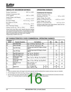
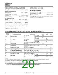
ABSOLUTE MAXIMUM RATINGS
OPERATING RANGES
Storage Temperature . . . . . . . . . . . . . .-65°C to +150°C
Commercial (C) Devices
Ambient Temperature with
Power Applied . . . . . . . . . . . . . . . . . .-55°C to +125°C
Ambient Temperature (T )
A
Operating in Free Air . . . . . . . . . . . . . . . 0°C to +75°C
Supply Voltage with Respect
to Ground . . . . . . . . . . . . . . . . . . . . . -0.5 V to +7.0 V
Supply Voltage (V ) with
CC
Respect to Ground (H/Q-15) . . . . . +4.75 V to +5.25 V
DC Input Voltage . . . . . . . . . . . .-0.5 V to V + 0.5 V
CC
Supply Voltage (V ) with
CC
Respect to Ground (H/Q-25) . . . . . . . +4.5 V to +5.5 V
DC Output or I/O Pin
Voltage . . . . . . . . . . . . . . . . . . .-0.5 V to V + 0.5 V
CC
Operating ranges define those limits between which the func-
tionality of the device is guaranteed.
Static Discharge Voltage . . . . . . . . . . . . . . . . . 2001 V
Latchup Current (T = 0°C to +75°C) . . . . . . . . 100 mA
A
Stresses above those listed under Absolute Maximum Ratings
may cause permanent device failure. Functionality at or above
these limits is not implied. Exposure to Absolute Maximum Rat-
ings for extended periods may affect device reliability.
Programming conditions may vary.
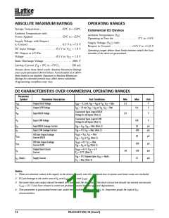
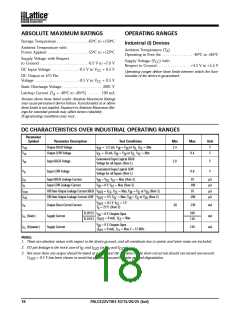
DC CHARACTERISTICS OVER COMMERCIAL OPERATING RANGES
Parameter
Symbol
Parameter Description
Output HIGH Voltage
Test Conditions
Min
Max
Unit
V
V
I
= -3.2 mA, V = V or V V = Min
IN IH IL, CC
2.4
OH
OH
V
Output LOW Voltage
I
= 16 mA, V = V or V V = Min
0.4
V
OL
OL
IN IH
IL, CC
Guaranteed Input Logical HIGH Voltage for all Inputs
(Note 1)
V
Input HIGH Voltage
Input LOW Voltage
2.0
V
V
IH
Guaranteed Input Logical LOW Voltage for all Inputs
(Note 1)
V
0.8
IL
I
Input HIGH Leakage Current
Input LOW Leakage Current
V = V , V = Max (Note 2)
IN CC CC
10
µA
µA
IH
I
V = 0 V, V = Max (Note 2)
-100
IL
IN
CC
Off-State Output Leakage
Current HIGH
I
V
= V , V = Max, V = V or V (Note 2)
10
µA
µA
mA
OZH
OUT CC CC
IN IL IH
Off-State Output Leakage
Current LOW
I
V
= 0 V, V = Max, V = V or V (Note 2)
-100
-130
OZL
OUT
CC
IN IL IH
Output Short-Circuit
Current
V
= 0.5 V, V = 5 V
CC
OUT
I
-30
SC
T = 25°C (Note 3)
A
H
Q
90
55
V = 0 V, Outputs Open
IN
I
Supply Current
mA
CC
(I = 0 mA), V = Max
OUT
CC
Notes:
1. These are absolute values with respect to the device ground, and all overshoots due to system and tester noise are included.
2. I/O pin leakage is the worst case of I and I (or I and I ).
IL OZL IH OZH
3. Not more than one output should be tested at a time, and the duration of the short-circuit test should not exceed one second.
V
= 0.5 V has been chosen to avoid test problems caused by tester ground degradation.
OUT
16
PALCE22V10H-15/25, Q-15/25 (Com’l)

 LATTICE [ LATTICE SEMICONDUCTOR ]