Specifications GAL20V8Z
GAL20V8ZD
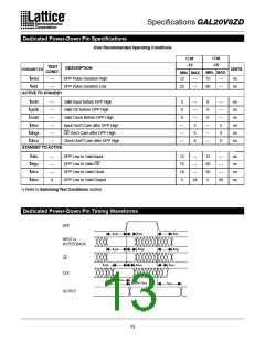
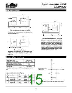
Power-Up Reset
Vcc (min.)
Vcc
t
su
t
wl
CLK
t
pr
Internal Register
Reset to Logic "0"
INTERNAL REGISTER
Q - OUTPUT
FEEDBACK/EXTERNAL
OUTPUT REGISTER
Device Pin
Reset to Logic "1"
asynchronous nature of system power-up, some conditions must
be met to provide a valid power-up reset of the GAL20V8Z/ZD.
First, the VCC rise must be monotonic. Second, the clock input
must be at static TTL level as shown in the diagram during power
up. The registers will reset within a maximum of tpr time. As in
normal system operation, avoid clocking the device until all input
and feedback path setup times have been met. The clock must
also meet the minimum pulse width requirements.
Circuitry within the GAL20V8Z/ZD provides a reset signal to all
registers during power-up. All internal registers will have their Q
outputs set low after a specified time (tpr, 1µs MAX). As a result,
the state on the registered output pins (if they are enabled) will
always be high on power-up, regardless of the programmed
polarity of the output pins. This feature can greatly simplify state
machine design by providing a known state on power-up. The
timing diagram for power-up is shown below. Because of the
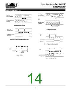
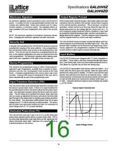
Input/Output Equivalent Schematics
PIN
PIN
Feedback
Vcc
Vcc
Tri-State
Control
Vcc
Vcc
ESD
Protection
Circuit
Data
Output
PIN
PIN
ESD
Protection
Circuit
Feedback
(To Input Buffer)
Typical Input
Typical Output
17

 LATTICE [ LATTICE SEMICONDUCTOR ]