Specifications GAL20V8Z
GAL20V8ZD
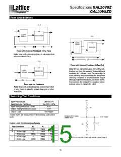
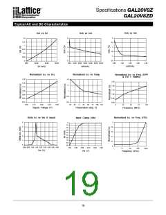
fmax Specifications
C L K
LOGIC
ARR AY
REGISTER
CLK
LOGIC
ARRAY
t
su
tc o
REGISTER
fmax with External Feedback 1/(tsu+tco)
Note: fmax with external feedback is calculated from
measured tsu and tco.
t
cf
pd
t
CLK
fmax with Internal Feedback 1/(tsu+tcf)
Note: tcf is a calculated value, derived by sub-
tracting tsu from the period of fmax w/internal
feedback (tcf = 1/fmax - tsu). The value of tcf is
used primarily when calculating the delay from
clocking a register to a combinatorial output
(through registered feedback), as shown above.
For example, the timing from clock to a combi-
natorial output is equal to tcf + tpd.
LOGIC
REGISTER
ARRAY
t
su + th
fmax with No Feedback
Note: fmax with no feedback may be less than 1/(twh
+ twl). This is to allow for a clock duty cycle of other
than 50%.
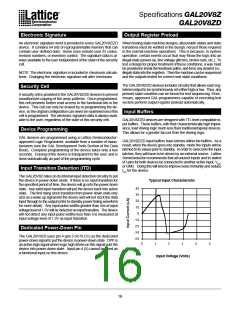
Switching Test Conditions
+5V
Input Pulse Levels
GND to 3.0V
3ns 10% – 90%
1.5V
Input Rise and Fall Times
Input Timing Reference Levels
Output Timing Reference Levels
R1
1.5V
Output Load
See Figure
3-state levels are measured 0.5V from steady-state active
level.
FROM OUTPUT (O/Q)
UNDER TEST
TEST POINT
C L*
Output Load Conditions (see figure)
R2
Test Condition
R1
300Ω
∞
R2
CL
A
390Ω
390Ω
390Ω
390Ω
390Ω
50pF
50pF
50pF
5pF
B
C
Active High
Active Low
Active High
Active Low
300Ω
∞
*CL INCLUDES TEST FIXTURE AND PROBE CAPACITANCE
300Ω
5pF
15

 LATTICE [ LATTICE SEMICONDUCTOR ]