Specifications GAL20V8Z
GAL20V8ZD
Electronic Signature
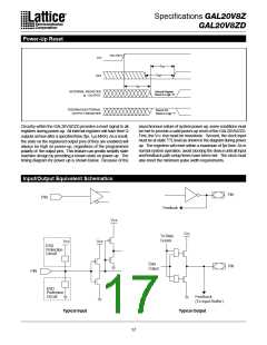
Output Register Preload
An electronic signature word is provided in every GAL20V8Z/ZD When testing state machine designs, all possible states and state
device. It contains 64 bits of reprogrammable memory that can transitions must be verified in the design, not just those required
contain user defined data. Some uses include user ID codes, in the normal machine operations. This is because, in system
revision numbers, or inventory control. The signature data is al- operation, certain events occur that may throw the logic into an
ways available to the user independent of the state of the security illegal state (power-up, line voltage glitches, brown-outs, etc.). To
cell.
test a design for proper treatment of these conditions, a way must
be provided to break the feedback paths, and force any desired (i.e.,
NOTE: The electronic signature is included in checksum calcula- illegal) state into the registers. Then the machine can be sequenced
tions. Changing the electronic signature will alter checksum.
and the outputs tested for correct next state conditions.
The GAL20V8Z/ZD devices includes circuitry that allows each reg-
istered output to be synchronously set either high or low. Thus, any
present state condition can be forced for test sequencing. If nec-
essary, approved GAL programmers capable of executing text
vectors perform output register preload automatically.
Security Cell
A security cell is provided in the GAL20V8Z/ZD devices to prevent
unauthorized copying of the array patterns. Once programmed,
this cell prevents further read access to the functional bits in the
device. This cell can only be erased by re-programming the de-
vice, so the original configuration can never be examined once this
cell is programmed. The electronic signature data is always avail-
able to the user, regardless of the state of this security cell.
Input Buffers
GAL20V8Z/ZD devices are designed with TTL level compatible in-
put buffers. These buffers, with their characteristically high imped-
ance, load driving logic much less than traditional bipolar devices.
This allows for a greater fan out from the driving logic.
Device Programming
GAL devices are programmed using a Lattice Semiconductor-
approved Logic Programmer, available from a number of manu-
facturers (see the GAL Development Tools Section of the Data
Book). Complete programming of the device takes only a few
seconds. Erasing of the device is transparent to the user, and is
done automatically as part of the programming cycle.
GAL20V8Z/ZD input buffers have latches within the buffers. As a
result, when the device goes into standby mode the inputs will be
latched to its values prior to standby. In order to overcome the input
latches, they will have to be driven by an external source. Lattice
Semiconductor recommends that all unused inputs and tri-stated
I/O pins for both devices be connected to another active input, VCC,
or GND. Doing this will tend to improve noise immunity and reduce
Input Transition Detection (ITD)
I
CC for the device.
The GAL20V8Z relies on its internal input detection circuitry to put
the device in power down mode. If there is no input transition for
the specified period of time, the device will go into the power down
state. Any valid input transition will put the device back into active
state. The first rising clock transition from power-down state only
acts as a wake up signal into the device and will not clock the data
input through to the output (refer to standby power timing waveform
for more detail). Any input pulse widths greater than 5ns at input
voltage level of 1.5V will be detected as input transition. The device
will not detect any input pulse widths less than 1ns measured at
input voltage level of 1.5V as input transition.
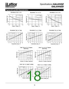
Typical Input Characteristic
40
30
20
10
0
- 1 0
- 2 0
- 3 0
Dedicated Power-Down Pin
The GAL20V8ZD uses pin 4 (pin 5 on PLCC) as the dedicated
power-down signal to put the device in power-down state. DPP is
an active high signal where logic high driven on this signal puts the
device into power-down state. Input pin 4 (5) cannot be used as
a functional input on this device.
- 4 0
0
1
2
3
4
5
Input Voltage (Volts)
16

 LATTICE [ LATTICE SEMICONDUCTOR ]