Pinout Information
LatticeECP2/M Family Data Sheet
Lattice Semiconductor
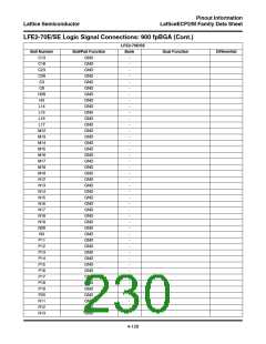
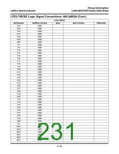
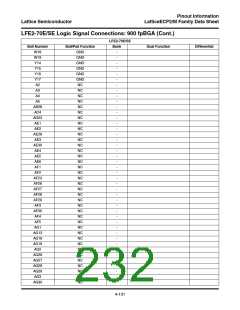
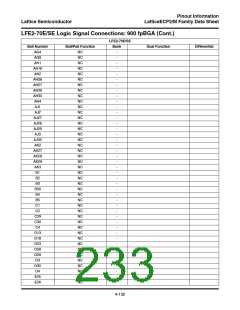
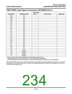
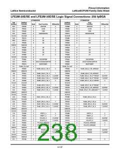
LFE2-70E/SE Logic Signal Connections: 900 fpBGA (Cont.)
LFE2-70E/SE
Ball Number
E27
E28
E29
E3
Ball/Pad Function
Bank
Dual Function
Differential
NC
NC
-
-
-
-
-
-
-
-
-
-
-
-
-
-
-
-
-
-
-
-
-
-
-
-
-
NC
NC
E30
E4
NC
NC
E5
NC
E6
NC
F25
F5
NC
NC
F6
NC
G6
NC
G7
NC
K10
K9
NC
NC
N27
N4
NC
NC
R1
NC
R2
NC
V27
V4
NC
NC
P22
P8
VCCPLL
VCCPLL
VCCPLL
VCCPLL
T22
Y7
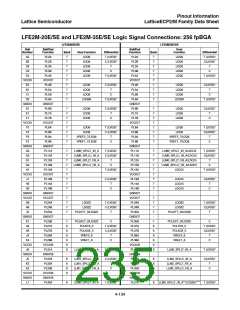
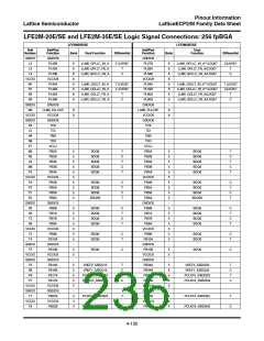
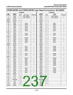
* Supports true LVDS. Other differential signals must be emulated with external resistors.
** These dedicated input pins can be used for GPLLs or GDLLs within the respective quadrant.
***Due to packaging bond out option, this DQS does not have all the necessary DQ pins bonded out for a full 8-bit data width.
Note: VCCIO and GND pads are used to determine the average DC current drawn by I/Os between GND/VCCIO connections, or between the
last GND/VCCIO in an I/O bank and the end of an I/O bank. The substrate pads listed in the Pin Table do not necessarily have a one to one
connection with a package ball or pin.
4-133

 LATTICE [ LATTICE SEMICONDUCTOR ]