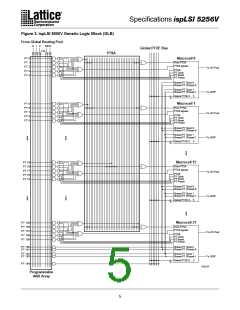
Specifications ispLSI 5256V
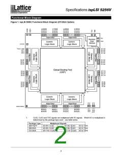
Functional Block Diagram
Figure 1. ispLSI 5256V Functional Block Diagram (272 BGA Option)
Input Bus
Input Bus
TDI
Boundary
Scan
Interface
TDO
Generic
Logic Block
Generic
Logic Block
VCCIO
1
I/O 0 / TOE
I/O 1
I/O 143
I/O 142
I/O 141
I/O 140
I/O 2
I/O 3
I/O 20
I/O 21
I/O 22
I/O 23
I/O 123
I/O 122
I/O 121
I/O 120
Global Routing Pool
(GRP)
I/O 119
I/O 118
I/O 117
I/O 116
I/O 24
I/O 25
I/O 26
I/O 27
I/O 99
I/O 98
I/O 97
I/O 96
I/O 44
I/O 45
I/O 46
I/O 47
Generic
Generic
Logic Block
Logic Block
Input Bus
Input Bus
GSET/GRST
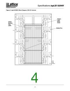
1.
CLK2, CLK3 and TOE signals are multiplexed with I/O signals. Which I/O is multiplexed is
determined by the package type used – see table below.
Package Type
Multplexed Signals
208 PQFP
208 BGA
272 BGA
I/O 89 / CLK2
I/O 89 / CLK2
I/O 119 / CLK2
I/O 98 / CLK3
I/O 98 / CLK3
I/O 131 / CLK3 I/O 0 / TOE
I/O 0 / TOE
I/O 0 / TOE
2

 LATTICE [ LATTICE SEMICONDUCTOR ]