ML13135
LANSDALE Semiconductor, Inc.
CIRCUIT DESCRIPTION
Mixers
The ML13135 is a complete dual conversion receiver. This
includes two local oscillators, two mixers, a limiting IF ampli-
fier and detector, and an op amp. It will provide a voltage
buffered RSSI with 70 dB of usable range, isolated tuning
diode and buffered LO output for PLL operation, and a sepa-
The first and second mixer are of similar design. Both are
double balanced to suppress the LO and input frequencies to
give only the sum and difference frequencies out. This config-
uration typically provides 40 to 60 dB of LO suppression. New
design techniques provide improved mixer linearity and third
order intercept without increased noise. The gain on the output
of the 1st mixer starts to roll off at about 20 MHz, so this
receiver could be used with a 21 MHz first IF. It is designed
for use with a ceramic filter, with an output impedance of 330
Ω. A series resistor can be used to raise the impedance for use
with a crystal filter, which typically has an input impedance of
4.0 kΩ. The second mixer input impedance is approximately
4.0 kΩ; it requires an external 360 Ω parallel resistor for use
with a standard ceramic filter.
rate V
pin for the first mixer and LO. Improvements have
CC
been made in the temperature performance of both the recov-
ered audio and the RSSI.
V
CC
Two separate V
lines enable the first LO and mixer to
CC
continue running while the rest of the circuit is powered down.
They also isolate the RF from the rest of the internal circuit.
Local Oscillators
The local oscillators are grounded collector Colpitts, which
can be easily crystal–controlled or VCO controlled with the
on–board varactor and external PLL. The first LO transistor is
internally biased, but the emitter is pinned–out and IQ can be
increased for high frequency or VCO operation. The collector
is not pinned out, so for crystal operation, the LO is generally
limited to 3rd overtone crystal frequencies; typically around 60
MHz. For higher frequency operation, the LO can be provided
externally as shown in Figure 16.
Limiting IF Amplifier and Detector
The limiter has approximately 110 dB of gain, which starts
rolling off at 2.0 MHz. Although not designed for wideband
operation, the bandwidth of the audio frequency amplifier has
been widened to 50 kHz, which gives less phase shift and
enables the receiver to run at higher data rates. However, care
should be taken not to exceed the bandwidth allowed by local
regulations.
The ML13135 is designed for use with an LC quadrature
detector, and does not have sufficient drive to be used with a
ceramic discriminator. The discriminators and the external
matching circuit will affect the distortion and recovered audio.
Buffer
An amplifier on the 1st LO output converts the single–ended
LO output to a differential signal to drive the mixer. Capacitive
coupling between the LO and the amplifier minimizes the
effects of the change in oscillator current on the mixer.
Buffered LO output is pinned–out at Pin 3 for use with a PLL,
RSSI/Op Amp
The Received Signal Strength Indicator (RSSI) on the
ML13135 has about 70 dB of range. The resistor needed to
translate the RSSI current to a voltage output has been includ-
ed on the internal circuit, which gives it a tighter tolerance. A
temperature compensated reference current also improves the
RSSI accuracy over temperature. On the ML13135, the op amp
is not connected internally and can be used for the RSSI or as
a data slicer (see Figure 17c).
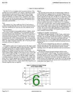
with a typical output voltage of 320 mVpp at V = 4.0 V and
CC
with a 5.1 k resistor from Pin 3 to ground. As seen in Figure
14, the buffered LO output varies with the supply voltage and
a smaller external resistor may be needed for low voltage oper-
ation. The LO buffer operates up to 60 MHz, typically. Above
60 MHz, the output at Pin 3 rolls off at approximately 6.0 dB
per octave. Since most PLLs require about 200 mVpp drive, an
external amplifier may be required.
Figure 14. Buffered LO Output Voltage
versus Supply Voltage
600
500
400
300
R
= 3.0 k
Ω
Pin3
R
= 5.1 kΩ
Pin3
200
100
2.5
3.0
3.5
4.0
4.5
5.0
5.5
V
, SUPPLY VOLTAGE (Vdc)
CC
Page 6 of 11
www.lansdale.com
Issue 0

 LANSDALE [ LANSDALE SEMICONDUCTOR INC. ]