ML13135
LANSDALE Semiconductor, Inc.
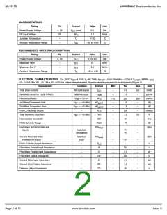
MAXIMUM RATINGS
Rating
Pin
4, 19
22
Symbol
(max)
Value
6.5
Unit
Vdc
Vrms
°C
Power Supply Voltage
RF Input Voltage
V
CC
RF
1.0
in
Junction Temperature
Storage Temperature Range
–
T
J
+150
–
T
stg
– 65 to +150
°C
RECOMMENDED OPERATING CONDITIONS
Rating
Power Supply Voltage
Maximum 1st IF
Pin
4, 19
–
Symbol
Value
2.0 to 6.0
21
Unit
Vdc
MHz
MHz
°C
V
CC
IF1
IF2
f
f
Maximum 2nd IF
–
3.0
Ambient Temperature Range
–
T
A
– 40 to + 85
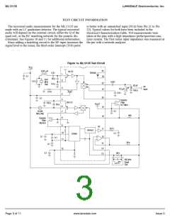
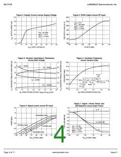
ELECTRICAL CHARACTERISTICS (T =25°C,V =4.0Vdc,f =49.7MHz,f
CC MOD
=1.0kHz,Deviation= 3.0kHz,f
1stLO
=39MHz,f
2nd
A
o
LO=10.245MHz, IF1=10.7MHz, IF2=455kHz, unless otherwisenoted. Allmeasurements performedinthetestcircuitofFigure1.)
Characteristic
Total Drain Current
Condition
No Input Signal
Matched Input
Symbol
Min
–
Typ
4.0
1.0
Max
6.0
–
Unit
I
mAdc
CC
Sensitivity (Input for 12 dB SINAD)
V
SIN
–
µVrms
Recovered Audio
V
= 1.0 mV
AF
mVrms
170
–
220
12
300
RF
O
1st Mixer Conversion Gain
V
= – 40 dBm
MX
MX
–
dB
RF
RF
gain1
gain2
2nd Mixer Conversion Gain
First LO Buffered Output
Total Harmonic Distortion
Demodulator Bandwidth
RSSI Dynamic Range
V
= – 40 dBm
–
–
–
–
–
13
100
1.2
50
–
–
dB
mVrms
%
–
V
LO
V
RF
= – 30 dBm
THD
BW
3.0
–
–
–
kHz
dB
RSSI
70
–
First Mixer 3rd Order Intercept
(Input)
TOI
dBm
Mix1
Matched
Unmatched
–
–
–17
–11
–
–
Second Mixer 3rd Order
Intercept (RF Input)
Matched
Input
TOI
dBm
Mix2
–
–
–
–
–
–
–
–
– 27
–
–
–
–
–
–
–
–
–
First LO Buffer Output Resistance
First Mixer Parallel Input Resistance
First Mixer Parallel Input Capacitance
First Mixer Output Impedance
–
–
–
–
–
–
–
R
Ω
Ω
LO
R
C
722
3.3
330
4.0
1.8
25
pF
Ω
ZO
Second Mixer Input Impedance
Second Mixer Output Impedance
Detector Output Impedance
Z
kΩ
kΩ
Ω
I
ZO
ZO
Page 2 of 11
www.lansdale.com
Issue 0

 LANSDALE [ LANSDALE SEMICONDUCTOR INC. ]