2.5 GB/S CWDM SFP TRANSCEIVER
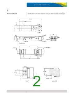
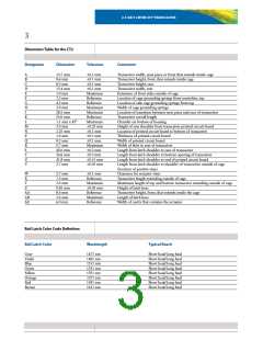
4
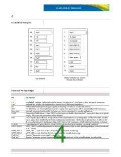
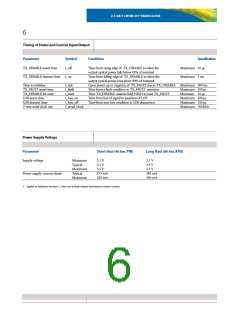
CT2 Electrical Pad Layout
20
1
VeeT
VeeT
19
18
17
16
15
14
13
12
11
2
TD-
Tx Fault
TD+
3
Tx Disable
4
MOD-DEF(2)
MOD-DEF(1)
VeeT
VccT
5
6
VccR
MOD-DEF(0)
Rate Select
7
VeeR
RD+
8
LOS
9
VeeR
VeeR
RD-
10
VeeR
Bottom of Board (As Viewed
through Top of Board)
Top of Board
Transceiver Pin Descriptions
Pin
Description
TD
TDb
Un-clocked, multirate, differential serial bit stream (155 Mb/s to 2.7 Gb/s) used to drive the optical transmitter.
Internally AC coupled and terminated via internal 100 Ω differential impedence.
RD
RDb
Rate_select
TxDIS
Differential received electrical signal capable of detecting 155 Mb/s to 2.7 Gb/s bit patterns.
The differential pair is internally biased and AC coupled. This signal requires 100 Ω external differential termination.
Internally monitored and available for future use. Can be customized for specific applications.
Transmitter Disable Input. A logic HIGH on this input pin disables the transmitter's laser so that there is no optical
output. If left open the transmitter will be disabled.
LOS
Loss of Signal (Open Collector). A logic HIGH on this output indicates an incoming signal level that is less than -25 dBm
but no greater than -31 dBm for the 40 km configuration and less than -34 dBm but no greater than -40 dBm for the
80 km configuration. LOS shall deassert (logic LOW) when a 3 dB (maximum), 0.5 dB (minimum) hysteresis is obtained.
Transmitter fault (Open collector). A logic HIGH indicates that the transmitter is in a fault condition.
MOD_DEF(0) is internally grounded to indicate the presence of the module. Must be pulled-up on host board with
10 KΩ resistor.
Tx_fault
MOD_DEF(0)
MOD_DEF(1)
MOD_DEF(2)
VccR,VccT
MOD_DEF(1) is the clock of the 2 wire interface for module monitoring.
MOD_DEF(2) is the data line of the 2 wire interface for module monitoring.
Receiver, Transmitter power supply, respectively
VeeR, VeeT
Receiver, Transmitter ground, respectively. The chassis ground and circuit ground isolation is configurable.

 JDSU [ JDSU ]