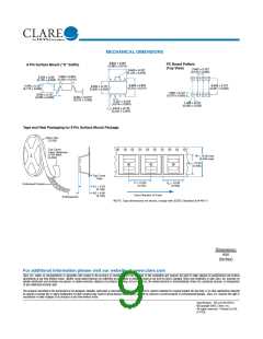
The LIA120
Where:
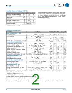
The LIA120 is an optically-coupled isolated linear error
amplifier. It integrates three of the most fundamental
elements necessary to make an isolated power supply:
a reference voltage, an error amplifier, and an isolated
coupling devices. It is functionally equivalent to a 431
type shunt regulator plus a linear optical amplifier.
• Gm = 1/ZOUT
which is ~ 3 Siemens
• CTRFB is approximately CTRForward = 0.02 nominally
CTRFB = K1, CTRFORWARD = K2, CTRFORWARD/CTRFB = K3
This calculation provides a more accurate gain
calculation but is only necessary when the voltage
divider resistor’s impedance is becoming close to the
optical output impedance of the shunt regulator.
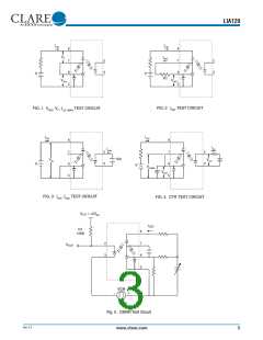
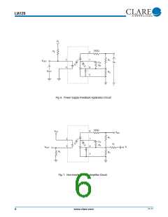
Powering the Isolated Input
The isolated input of the LIA120 is powered through the
LED pin (pin 8) via the part to it’s isolated ground at pin 5.
The typical operating current of the device is determined
by the output voltage and current requirements as well as
the CTR of the linear optocoupler. For Figure 7, the LED
current requirement is set by the following equation.
Compensation
The LIA120 is relatively easy to compensate but two
factors must be considered when analyzing the circuit.
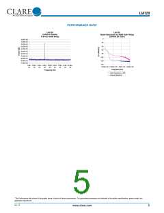
The frequency response of the LIA120 can be as high
as 40kHz, but must be limited because of the closed
loop optical feedback to the input signal. In the localized
optical feedback there are two poles to consider, the 431
dominant pole and the linear optical coupler pole. The
open loop gain of the optical loop (for the application
diagram) is:
Vout, bias
RL • K1
ILED
The output voltage is typically constrained by the user to
satisfy the design requirements of the application circuit.
Design considerations must also take into account that
RL affects the total gain and that CTR gains vary with
process. Nominally the LED current should be around
1-2mA but can be as high as 10-15mA if the user
requires.
CTRFB R1 R2
The open loop gain is affected by the selection of R1
and R2 and without any compensation the circuit may
oscillate. The addition of a compensation network (Cc
and Rc) control the maximum bandwidth so that open
loop gain is rolling off long before the optical pole causes
the circuit to oscillate. The optical pole is at ~180kHz so
the bandwidth is typically limited to less than 40kHz.
LED current is limited by the resistor in series with pin 8,
the LED pin, to the supply and is typically 10-100 ohms
for operating currents of 1-2mA. The minimum operating
voltage of 2.74V for the LIA120 from pin 8 to pin 5 is
based on the sum of the voltage drop of the LED and
the operational voltage headroom of the 431. Minimum
operating voltage for the application circuit is therefore
the sum of the LIA120 minimum operating voltage plus
the voltage drop of the current limiting resistor For a
design with 1mA of LED current and a current limiting
resistor of 100 ohms, the minimum operating voltage is
calculated to be 2.74 + (0.001)(100) = 2.84V.
While there is flexibility in the part to change the
compensation technique, the upper limit on frequency
response is generally desired to be such that the circuit
will not oscillate for a large selection of R1 and R2
Therefore the compensation capacitor should not be less
than 100pF which gives adequate bandwidth for most
designs. The bandwidth through the part will be:
R1 R2
Feedback
RLED Cc
R1 R2
Setting the gain for the LIA120 is accomplished simply
by setting two resistors. The application circuit in
Figure 6 shows a resistor divider feeding the FB pin, so
the operating conditions for the gain are governed by:
P1
Where:
P1 max is 1kHz (6.28krad/s) due to the internal
compensation of the 431.
CTR is the current transfer ratio of the feedback
optocoupler (0.001-0.003).
R1
R2
R1
1
K3
RLED is the combined impedance of the limiting resistor
and the LED resistance (25 ohms) and Gm is the
transconductance of the 431 (3 Siemens).
K3 is taken from the datasheet as 1 nominally. The ac
gain of the setup can be represented by:
However, since some of these elements vary over
operating conditions and temperature, the bandwidth
should be practically limited to less than 40kHz to avoid
oscillations, which is the value computed by 100pF.
m
VOUT VIN
•
m
Rev. 2.0
www.clare.com
7

 IXYS [ IXYS CORPORATION ]