LIA120
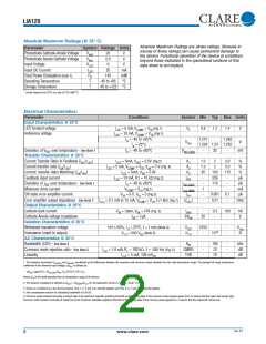
Absolute Maximum Ratings (@ 25˚ C)
Absolute Maximum Ratings are stress ratings. Stresses in
excess of these ratings can cause permanent damage to
the device. Functional operation of the device at conditions
beyond those indicated in the operational sections of this
data sheet is not implied.
Parameter
Symbol Ratings Units
Photodiode Cathode-Anode Voltage
Photodiode Anode-Cathode Voltage
Input Voltage
VKAO
VAKO
VLED
ILED
PD
20
0.5
9
20
145
V
V
V
mA
mW
°C
Input DC Current
Total Power Dissipation (note 1)
Operating Temperature
Storage Temperature
T
-40 to +85
T
-40 to +125 °C
1
Derate linearly from 25°C at a rate of 2.42 mW/ °C.
Electrical Characteristics:
Parameter
Input Characteristics @ 25°C
LED forward voltage
Conditions
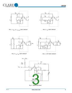
ILED = 5 mA, VCOMP = VFB (Fig.1)
VF
0.8
1.2
1.4
V
Reference voltage
ILED = 10 mA, VCOMP = VFB (Fig.1)
TA = -40 to +85°C
TA = 25°C
1.210
1.228 1.24 1.252
1.265
VREF
V
Deviation of VREF over temperature - See Note 1
TA = -40 to +85°C
VREF (DEV)
32
mV
Transfer Characteristics @ 25°C
Current Transfer Ratio in Feedback (IREF
/ILED
)
ILED = 5mA, VREF = 0.5V (Fig.2)
ILED = 5 mA, VCOMP = VFB, VKA = 5 V (Fig. 4)
ILED = 5mA, VKA = 5.0V
K1
K2
K3
1.0
1.0
85
1
2
2
100
226
110
3.0
3.0
115
%
%
%
µA
µA
Current transfer ratio (IKA
/ILED
)
Current Transfer Ratio Matching (IKA
/IREF
)
Feedback input current
Deviation of IREF over temperature - See Note 1
Minimum drive current
ILED = 10 mA, R1 = 10 kΩ (Fig.2)
TA = -40 to +85°C
IREF
IREF (DEV)
ILED (MIN)
IOFF
VCOMP = VFB (Fig.1)
VIN = 6 V, VFB = 0 (Fig.3)
mA
µA
Off-state error amplifier current
0.001 0.1
Error amplifier output impedance - See Note 2 ILED = 0.1 mA to 15 mA, VCOMP = VFB, f<1 kHz (Fig.1)
IZOUT
I
0.21
Ohm
Output Characteristics @ 25°C
Cathode dark current
VIN = Open, VKA = 10V (Fig. 3)
IKA = 1µA
IKAO
BVKA
20
0.3
100
nA
V
Cathode-Anode voltage breakdown
Isolation Characteristics @ 25°C
Withstand insulation voltage
Resistance (input to output)
AC Characteristics @ 25°C
Bandwidth (LED) - See Note 4
Common mode rejection ratio - See Note 5
Linearity
RH ≤ 50%, TA = 25°C, t = 1 min (Note 3)
VISO
RI-O
3750
Vrms
Ω
VI-O = 500 VDC (Note 3)
1012
BW
CMRR
THD
100
70
70
kHz
dB
dB
ILED = 1.0 mA, RL = 100 kΩ, f = 100 Hz (Fig. 5)
ILED = 5 mA, 100 mVPP
1. The deviation parameters VREF(DEV) and IREF(DEV) are defined as the differences between the maximum and minimum values obtained over the rated temperature range. The average full-range temperature
coefficient of the reference input voltage, ∆VREF, is defined as:
|∆VREF| (ppm/°C) = {VREF (DEV)/VREF (TA 25°C)} X 106 / ∆TA
where ∆TA is the rated operating free-air temperature range of the device.
2. The dynamic impedance is defined as |ZOUT| = ∆VCOMP/∆ILED, for the application circuit in Figure 6, |Zout| = K1R1
3. Device is considered as a two terminal device: Pins 1, 2, 3 and 4 are shorted together and Pins 5, 6, 7 and 8 are shorted together.
4. See compensation section for calculating bandwidth of LIA120.
5. Common mode transient immunity at output high is the maximum tolerable (positive) dVcm/dt on the leading edge of the common mode impulse signal, Vcm, to assure that the output will remain high.
Common mode transient immunity at output low is the maximum tolerable (negative) dVcm/dt on the trailing edge of the common pulse signal,Vcm, to assure that the output will remain low.
Rev. 2.0
2

 IXYS [ IXYS CORPORATION ]