AS7C252MNTF18A
®
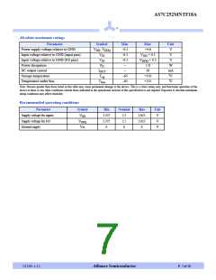
Absolute maximum ratings
Parameter
Power supply voltage relative to GND
Input voltage relative to GND (input pins)
Input voltage relative to GND (I/O pins)
Power dissipation
Symbol
, V
Min
–0.5
–0.5
–0.5
–
Max
Unit
V
+4.6
V
DD
DDQ
V
V
+ 0.5
DD
V
V
IN
IN
V
V
+ 0.5
DDQ
P
1.8
W
D
DC output current
I
–
20
mA
OUT
o
Storage temperature
T
–65
–65
+150
+135
C
stg
o
Temperature under bias
T
C
bias
Note: Stresses greater than those listed in this table may cause permanent damage to the device. This is a stress rating only, and functional operation of the
device at these or any other conditions outside those indicated in the operational sections of this specification is not implied. Exposure to absolute maximum
rating conditions may affect reliability.
Recommended operating conditions
Parameter
Supply voltage for inputs
Supply voltage for I/O
Ground supply
Symbol
VDD
Min
2.375
2.375
0
Nominal
Max
2.625
2.625
0
Unit
V
2.5
2.5
0
VDDQ
Vss
V
V
1/17/05, v 1.1
Alliance Semiconductor
P. 7 of 18

 ISSI [ INTEGRATED SILICON SOLUTION, INC ]