AS7C252MNTF18A
®
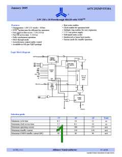
Functional Description
The AS7C252MNTF18A family is a high performance CMOS 32 Mbit synchronous Static Random Access Memory (SRAM)
organized as 2,097,152 words × 18 bits and incorporates a LATE Write.
™
This variation of the 32Mb+ synchronous SRAM uses the No Turnaround Delay (NTD ) architecture, featuring an enhanced
write operation that improves bandwidth over flowthrough burst devices. In a normal flowthrough burst device, the write data,
command, and address are all applied to the device on the same clock edge. If a read command follows this write command,
the system must wait for one 'dead' cycle for valid data to become available. This dead cycle can significantly reduce overall
bandwidth for applications requiring random access or read-modify-write operations.
™
NTD devices use the memory bus more efficiently by introducing a write latency which matches the one-cycle flow-
through read latency. Write data is applied one cycle after the write command and address, allowing the read pipeline to clear.
™
With NTD , write and read operations can be used in any order without producing dead bus cycle.
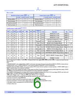
Assert R/W low to perform write cycles. Byte write enable controls write access to specific bytes, or can be tied low for full 18
bit writes. Write enable signals, along with the write address, are registered on a rising edge of the clock. Write data is applied
to the device one clock cycle later. Unlike some asynchronous SRAMs, output enable OE does not need to be toggled for write
operations; it can be tied low for normal operations. Outputs go to a high impedance state when the device is de-selected by
any of the three chip enable inputs.
Use the ADV (burst advance) input to perform burst read, write and deselect operations. When ADV is high, external addresses, chip
select, R/W pins are ignored, and internal address counters increment in the count sequence specified by the LBO control. Any
device operations, including burst, can be stalled using the CEN=1, the clock enable input.
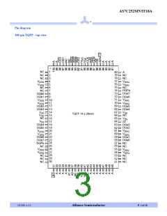
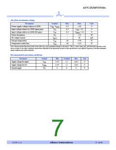
The AS7C252MNTF18A operates with a 2.5V ± 5% power supply for the device core (V ). These devices are available in
DD
100-pin TQFP package.
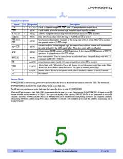
TQFP Capacitance
Parameter
Input capacitance
I/O capacitance
*Guaranteed not tested
Symbol
Signals
Address and control pins
I/O pins
Test conditions
V = 0V
Max
Unit
pF
*
C
5
7
IN
in
*
C
V = V = 0V
pF
I/O
in
out
TQFP thermal resistance
Description
Symbol
Typical
Units
Conditions
1 layer
4 layer
θ
40
22
°C/W
°C/W
Thermal resistance
(junction to ambient)
JA
Test conditions follow standard test
methods and procedures for
measuring thermal impedance, per
EIA/JESD51
1
θ
JA
Thermal resistance
(junction to top of case)
θ
8
°C/W
1
JC
1 This parameter is sampled.
1/17/05, v 1.1
Alliance Semiconductor
P. 4 of 18

 ISSI [ INTEGRATED SILICON SOLUTION, INC ]