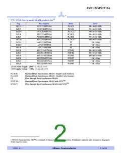
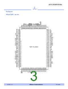
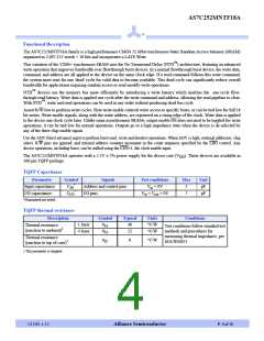
AS7C252MNTF18A
®
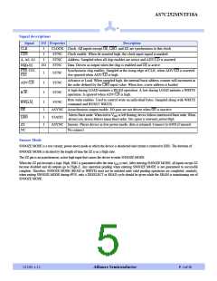
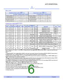
Burst order
Interleaved burst order (LBO = 1)
A1A0 A1A0 A1A0 A1A0
Linear burst order (LBO = 0)
A1A0 A1A0 A1A0 A1A0
Starting address
First increment
0 0
0 1
0 1
0 0
1 1
1 0
1 0
1 1
0 0
0 1
1 1
1 0
0 1
0 0
Starting Address
First increment
0 0
0 1
0 1
1 0
1 1
0 0
1 0
1 1
0 0
0 1
1 1
0 0
0 1
1 0
Second increment 1 0
Third increment 1 1
Second increment 1 0
Third increment
1 1
Synchronous truth table[5,6,7,8,9,11]
Address
CE0 CE1 CE2 ADV/LD R/W
BWn
OE CEN source
CLK
Operation
DQ
High-Z
High-Z
High-Z
High-Z
Q
Notes
H
X
X
X
L
X
X
L
X
H
X
X
L
L
L
L
H
L
H
L
H
L
H
L
X
X
X
X
H
X
H
X
L
X
X
X
X
X
X
X
X
L
X
X
X
X
L
L
L
L
L
L
L
L
L
L
L
L
NA
NA
NA
NA
L to H
L to H
L to H
L to H
DESELECT Cycle
DESELECT Cycle
DESELECT Cycle
X
H
X
H
X
H
X
H
CONTINUE DESELECT Cycle
READ Cycle (Begin Burst)
READ Cycle (Continue Burst)
1
External L to H
Next L to H
X
L
X
L
L
Q
1,10
2
H
H
X
X
X
External L to H NOP/DUMMY READ (Begin Burst) High-Z
X
L
X
L
Next L to H DUMMY READ (Continue Burst) High-Z 1,2,10
External L to H
WRITE CYCLE (Begin Burst)
D
D
3
X
L
X
L
X
L
L
Next L to H WRITE CYCLE (Continue Burst)
1,3,10
H
External L to H NOP/WRITE ABORT (Begin Burst) High-Z 2,3
1,2,3,
X
X
X
H
X
H
X
X
L
Next L to H WRITE ABORT (Continue Burst)
High-Z
10
X
X
X
X
X
X
H
Current L to H
INHIBIT CLOCK
-
4
Key: X = Don’t Care, H = HIGH, L = LOW. BWn = H means all byte write signals (BWa, BWb) are HIGH. BWn = L means one or more byte write
signals are LOW.
Notes:
1 CONTINUE BURST cycles, whether READ or WRITE, use the same control inputs. The type of cycle performed (READ or WRITE) is chosen in the ini-
tial BEGIN BURST cycle. A CONINUE DESELECT cycle can only be entered if a DESELECT CYCLE is executed first.
2 DUMMY READ and WRITE ABORT cycles can be considered NOPs because the device performs no external operation. A WRITE ABORT means a
WRITE command is given, but no operation is performed.
3 OE may be wired LOW to minimize the number of control signal to the SRAM. The device will automatically turn off the output drivers during a WRITE
cycle. OE may be used when the bus turn-on and turn-off times do not meet an application’s requirements.
4 If an INHIBIT CLOCK command occurs during a READ operation, the DQ bus will remain active (Low-Z). If it occurs during a WRITE cycle, the bus will
remain in High-Z. No WRITE operations will be performed during the INHIBIT CLOCK cycle.
5 BWa enables WRITEs to byte “a” (DQa pins); BWb enables WRITEs to byte “b” (DQb pins).
6 All inputs except OE and ZZ must meet setup and hold times around the rising edge (LOW to HIGH) of CLK.
7 Wait states are inserted by setting CEN HIGH.
8 This device contains circuitry that will ensure that the outputs will be in High-Z during power-up.
9 The device incorporates a 2-bit burst counter. Address wraps to the initial address every fourth BURST CYCLE.
10 The address counter is incremented for all CONTINUE BURST cycles.
11 ZZ pin is always Low.
1/17/05, v 1.1
Alliance Semiconductor
P. 6 of 18

 ISSI [ INTEGRATED SILICON SOLUTION, INC ]