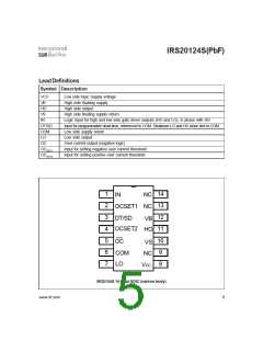
IRS20124S(PbF)
Recommended Operating Conditions
For Proper operation, the device should be used within the recommended conditions. The Vs and COM
offset ratings are tested with all supplies biased at 15V differential.
Symbol
VB
Definition
High side floating supply absolute voltage
High side floating supply offset voltage
High side floating output voltage
Low side fixed supply voltage
Low side output voltage
Logic input voltage
OC pin input voltage
OCSET1 pin input voltage
OCSET2 pin input voltage
Ambient Temperature
Min.
Max.
Vs+18
200
VB
18
VCC
VCC
VCC
VCC
VCC
125
Units
V
V
V
V
V
V
V
V
Vs+10
VS
VHO
VCC
VLO
VIN
VOC
VOCSET1
VOCSET2
TA
Note 1
Vs
10
0
0
0
0
0
-40
V
°C
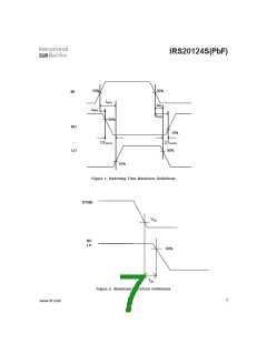
Note 1: Logic operational for V equal to -8V to 200V. Logic state held for V equal to -8V to -V .
S S BS
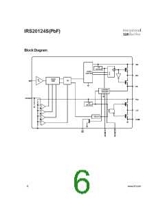
Dynamic Electrical Characteristics
V
BIAS
(V , V ) = 15V, C = 1nF and T = 25°C unless otherwise specified. Figure 2 shows the timing definitions.
CC BS
L
A
Symbol
Definition
Min. Typ. Max. Units Test Conditions
t
High & low side turn-on propagation delay
High & low side turn-off propagation delay
Turn-on rise time
—
—
—
—
—
—
60
60
80
80
VS=0V
on
t
VS=200V
off
t
25
15
140
280
40
35
200
—
r
t
Turn-off fall time
Shutdown propagation delay
Propagation delay time from Vs>Vsoc+ to OC
f
tsd
toc
OCSET1=3.22V
OCSET2=1.20V
nsec
twoc min OC pulse width
—
—
100
200
—
—
toc filt
OC input filter time
Deadtime: LO turn-off to HO turn-on (DTLO-HO
& HO turn-off to LO turn-on (DTHO-LO
Deadtime: LO turn-off to HO turn-on (DTLO-HO
& HO turn-off to LO turn-on (DTHO-LO
Deadtime: LO turn-off to HO turn-on (DTLO-HO
& HO turn-off to LO turn-on (DTHO-LO
Deadtime: LO turn-off to HO turn-on (DTLO-HO
& HO turn-off to LO turn-on (DTHO-LO)VDT= VDT4 15
DT1
)
)
0
15
25
35
45
40
50
60
70
VDT>VDT1
DT2
DT3
DT4
)
)
5
VDT1>VDT> VDT2
VDT2>VDT> VDT3
VDT3>VDT> VDT4
)
)
10
)
www.irf.com
3

 INFINEON [ Infineon ]