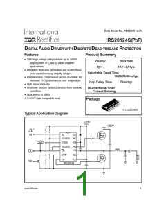
IRS20124S(PbF)
Description
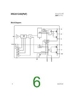
The IRS20124S is a high voltage, high speed power MOSFET driver with internal dead-time and shutdown
functions specially designed for Class D audio amplifier applications.
The internal dead time generation block provides accurate gate switch timing and enables tight dead-time
settings for better THD performances.
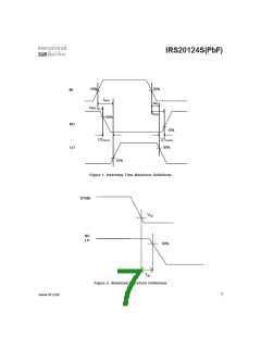
In order to maximize other audio performance characteristics, all switching times are designed for immunity
from external disturbances such as VCC perturbation and incoming switching noise on the DT pin. Logic
inputs are compatible with LSTTL output or standard CMOS down to 3.0V without speed degradation. The
output drivers feature high current buffers capable of sourcing 1.0A and sinking 1.2A. Internal delays are
optimized to achieve minimal dead-time variations. Proprietary HVIC and latch immune CMOS technologies
guarantee operation down to Vs= –4V, providing outstanding capabilities of latch and surge immunities with
rugged monolithic construction.
Absolute Maximum Ratings
Absolute maximum ratings indicate sustained limits beyond which damage to the device may occur. All voltage parameters
are absolute voltages referenced to COM. All currents are defined positive into any lead. The thermal resistance and power
dissipation ratings are measured under board mounted and still air conditions.
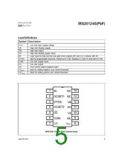
Symbol
Definition
High side floating supply voltage
High side floating supply voltage
High side floating output voltage
Low side fixed supply voltage
Low side output voltage
Input voltage
OC pin input voltage
OCSET1 pin input voltage
OCSET2 pin input voltage
Allowable Vs voltage slew rate
Maximum power dissipation
Thermal resistance, Junction to ambient
Junction Temperature
Storage Temperature
Lead temperature (Soldering, 10 seconds)
Min.
-0.3
VB-20
Vs-0.3
-0.3
-0.3
-0.3
-0.3
-0.3
-0.3
-
Max.
220
VB+0.3
VB+0.3
20
Vcc+0.3
Vcc+0.3
Vcc+0.3
Vcc+0.3
Vcc+0.3
50
Units
V
V
V
V
V
V
V
V
V
V/ns
W
°C/W
°C
°C
°C
VB
V
s
VHO
VCC
VLO
VIN
VOC
VOCSET1
VOCSET2
dVs/dt
Pd
RthJA
TJ
-
-
-
1.25
100
150
150
TS
TL
-55
-
300
2
www.irf.com

 INFINEON [ Infineon ]