IRLML6402PbF-1
Electrical Characteristics @ TJ = 25°C (unless otherwise specified)
Parameter
Min. Typ. Max. Units
-20 ––– –––
Conditions
V(BR)DSS
Drain-to-Source Breakdown Voltage
V
VGS = 0V, ID = -250μA
ΔV(BR)DSS/ΔTJ Breakdown Voltage Temp. Coefficient
––– -0.009 ––– V/°C Reference to 25°C, ID = -1mA
––– 0.050 0.065
––– 0.080 0.135
-0.40 -0.55 -1.2
6.0 ––– –––
––– ––– -1.0
––– ––– -25
––– ––– -100
––– ––– 100
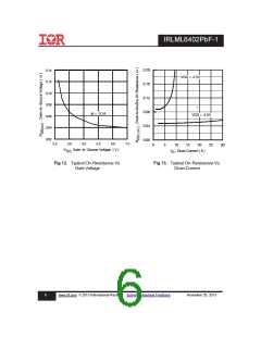
VGS = -4.5V, ID = -3.7A
VGS = -2.5V, ID = -3.1A
VDS = VGS, ID = -250μA
VDS = -10V, ID = -3.7A
VDS = -20V, VGS = 0V
VDS = -20V, VGS = 0V, TJ = 70°C
VGS = -12V
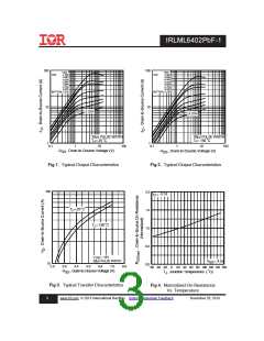
RDS(on)
Static Drain-to-Source On-Resistance
Ω
VGS(th)
gfs
Gate Threshold Voltage
V
S
Forward Transconductance
IDSS
Drain-to-Source Leakage Current
µA
nA
Gate-to-Source Forward Leakage
Gate-to-Source Reverse Leakage
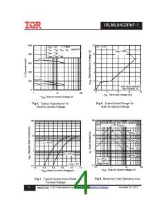
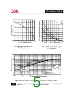
Total Gate Charge
IGSS
VGS = 12V
Qg
––– 8.0
12
ID = -3.7A
Qgs
Qgd
td(on)
tr
Gate-to-Source Charge
Gate-to-Drain ("Miller") Charge
Turn-On Delay Time
Rise Time
––– 1.2 1.8
––– 2.8 4.2
––– 350 –––
––– 48 –––
––– 588 –––
––– 381 –––
––– 633 –––
––– 145 –––
––– 110 –––
nC VDS = -10V
VGS = -5.0V
VDD = -10V
ID = -3.7A
ns
td(off)
tf
Turn-Off Delay Time
Fall Time
RG = 89Ω
RD = 2.7Ω
VGS = 0V
Ciss
Coss
Crss
Input Capacitance
Output Capacitance
pF
VDS = -10V
ƒ = 1.0MHz
Reverse Transfer Capacitance
Source-Drain Ratings and Characteristics
Parameter
Continuous Source Current
(Body Diode)
Min. Typ. Max. Units
Conditions
D
S
IS
MOSFET symbol
showing the
-1.3
-22
––– –––
––– –––
A
G
ISM
Pulsed Source Current
(Body Diode)
integral reverse
p-n junction diode.
VSD
trr
Diode Forward Voltage
Reverse Recovery Time
Reverse RecoveryCharge
––– ––– -1.2
V
TJ = 25°C, IS = -1.0A, VGS = 0V
––– 29
––– 11
43
17
ns
TJ = 25°C, IF = -1.0A
Qrr
nC di/dt = -100A/μs
Notes:
Surface mounted on 1" square single layer 1oz. copper FR4 board,
Repetitive rating; pulse width limited by
max. junction temperature.
steady state.
Pulse width ≤ 400μs; duty cycle ≤ 2%.
Starting TJ = 25°C, L = 1.65mH
RG = 25Ω, IAS = -3.7A.
** For recommended footprint and soldering techniques refer to application note #AN-994.
2
www.irf.com © 2013 International Rectifier Submit Datasheet Feedback
November 25, 2013

 INFINEON [ Infineon ]