IRL520N
200
160
120
80
I
D
TOP
2.4A
4.2A
6.0A
15V
BO TTO M
DRIVER
L
V
D S
D.U .T
R
G
+
V
DD
-
I
A
AS
10V
Ω
0.01
t
p
40
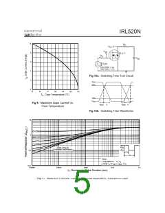
Fig 12a. Unclamped Inductive Test Circuit
0
A
25
50
75
100
125
150
175
V
Starting T , Junction Tem perature (°C)
(BR)DSS
J
t
p
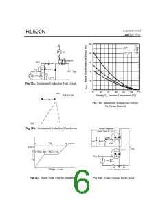
Fig 12c. Maximum Avalanche Energy
Vs. Drain Current
I
AS
Current Regulator
Fig 12b. Unclamped Inductive Waveforms
Same Type as D.U.T.
50KΩ
.2µF
12V
.3µF
Q
G
+
5.0 V
V
DS
D.U.T.
-
Q
Q
GD
GS
V
GS
V
G
3mA
I
I
D
G
Charge
Current Sampling Resistors
Fig 13a. Basic Gate Charge Waveform
Fig 13b. Gate Charge Test Circuit

 INFINEON [ Infineon ]