IRF9Z24N
1 2
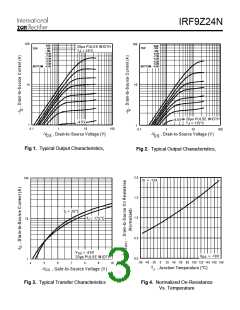
RD
VDS
VGS
D.U.T.
9
RG
-
+
VDD
-10V
6
Pulse Width ≤ 1 µs
Duty Factor ≤ 0.1 %
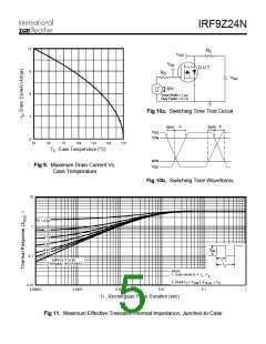
Fig 10a. Switching Time Test Circuit
3
t
t
r
t
t
f
d(on)
d(off)
V
GS
10%
0
A
1 7 5
2 5
5 0
7 5
1 0 0
1 2 5
1 5 0
TC , Case Temperature (°C)
90%
Fig 9. Maximum Drain Current Vs.
V
DS
Case Temperature
Fig 10b. Switching Time Waveforms
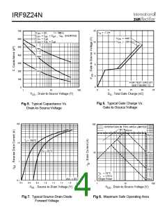
1 0
D
=
0 .5 0
0 .2 0
1
0 .1 0
0 .0 5
P
0 .0 2
0 .0 1
DM
0. 1
t
S IN G LE P U L S E
(T H E R M A L R E S P O N S E )
1
t
2
Notes:
1. D uty factor D
=
t
/ t
1
2
2. Pea k T = P
x Z
+ T
C
DM
J
th JC
A
0 . 0 1
0 . 0 0 0 0 1
0 . 0 0 0 1
0 . 0 0 1
0 . 0 1
0. 1
1
t1 , Rectan gular Pulse Duratio n (sec)
Fig 11. Maximum Effective Transient Thermal Impedance, Junction-to-Case

 INFINEON [ Infineon ]