IR11682S
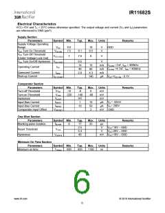
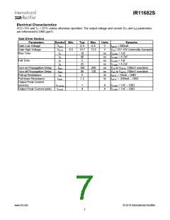
Electrical Characteristics
VCC=15V and TA = 25°C unless otherwise specified. The output voltage and current (VO and IO) parameters
are referenced to GND (pin7).
Gate Driver Section
Parameters
Gate Low Voltage
Gate High Voltage
Rise Time
Symbol Min.
VGLO
Typ.
0.3
10.7
10
80
5
25
100
80
5
1.2
Max.
0.5
13.5
Units
V
V
ns
ns
ns
ns
ns
ns
Ω
Remarks
IGATE = 200mA
VCC=12V-18V (internally clamped)
CLOAD = 1nF
CLOAD = 4.7nF
CLOAD = 1nF
VGTH
tr1
8.5
tr2
tf1
tf2
tDon
tDoff
rup
Fall Time
CLOAD = 4.7nF
Turn on Propagation Delay
Turn off Propagation Delay
Pull up Resistance
Pull down Resistance
Output Peak Current
(source)
200
120
VDS to VGATE -100mV overdrive
VDS to VGATE -100mV overdrive
IGATE = 15mA – GBD
IGATE = -200mA – GBD
rdown
Ω
IO source
IO sink
1
4
A
A
CLOAD = 1nF – GBD
CLOAD = 1nF – GBD
Output Peak Current (sink)
www.irf.com
© 2010 International Rectifier
7

 INFINEON [ Infineon ]