ISL88731C
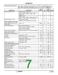
Electrical Specifications DCIN = CSSP = CSSN = 18V, CSOP = CSON = 12V, VDDP = 5V, BOOT-PHASE = 5.0V,
GND = PGND = 0V, CVDDP = 1µF, IVDDP = 0mA, T = -10°C to +100°C. Boldface limits
A
apply over the operating temperature range, -10°C to +100°C. (Continued)
MIN
MAX
PARAMETER
SWITCHING REGULATOR
Frequency
CONDITIONS
(Note 8)
TYP
(Note 8) UNITS
330
170
400
290
0
440
400
2
kHz
µA
µA
Ω
BOOT Supply Current
PHASE Input Bias Current
UGATE On-Resistance Low
UGATE On-Resistance High
LGATE On-Resistance High
LGATE On-Resistance Low
Dead Time
UGATE High
V
= 28V, V
CSON
= V = 20V
PHASE
DCON
UGATE
UGATE
LGATE
LGATE
I
I
I
I
= -100mA (Note 7)
= 10mA (Note 7)
= +10mA (Note 7)
= -100mA (Note 7)
0.9
1.4
1.4
0.9
50
1.6
2.5
2.5
1.6
80
Ω
Ω
Ω
Falling UGATE to rising LGATE or
falling LGATE to rising UGATE
35
ns
ERROR AMPLIFIERS
GMV Amplifier Transconductance
GMI Amplifier Transconductance
GMS Amplifier Transconductance
GMI/GMS Saturation Current
GMV Saturation Current
200
40
250
50
300
60
µA/V
µA/V
µA/V
µA
40
50
60
15
21
25
10
17
30
µA
ICOMP, VCOMP Clamp Voltage
LOGIC LEVELS
0.25V < V
ICOMP, VCOMP
< 3.5V
200
300
400
mV
SDA/SCL Input Low Voltage
SDA/SCL Input High Voltage
SDA/SCL Input Bias Current
SDA, Output Sink Current
VDDSMB = 2.7V to 5.5V
VDDSMB = 2.7V to 5.5V
VDDSMB = 2.7V to 5.5V
0.8
1
V
V
2
-1
7
µA
mA
V
= 0.4V
15
SDA
SMBus Timing Specifications VDDSMB = 2.7V to 5.5V.
PARAMETER
SYMBOL
CONDITIONS
MIN TYP MAX UNITS
SMBus Frequency
Bus Free Time
FSMB
10
4.7
4
100
kHz
µs
µs
µs
µs
ns
ns
ms
µs
µs
s
t
BUF
Start Condition Hold Time from SCL
Start Condition Setup Time from SCL
Stop Condition Setup Time from SCL
SDA Hold Time from SCL
SDA Setup Time from SCL
SCL Low Timeout (Note 6)
SCL Low Period
t
HD:STA
t
4.7
4
SU:STA
SU:STO
HD:DAT
t
t
300
250
22
4.7
4
t
SU:DAT
t
25
30
TIMEOUT
t
LOW
SCL High Period
t
HIGH
Maximum Charging Period without an SMBus Write to
ChargeVoltage or ChargeCurrent Register
140 180 220
NOTES:
6. If SCL is low for longer than the specified time, the charger is disabled.
7. Limits established by characterization and are not production tested.
8. Parameters with MIN and/or MAX limits are 100% tested at +25°C, unless otherwise specified. Temperature limits established
by characterization and are not production tested.
FN6978.0
March 8, 2010
8

 INTERSIL [ Intersil ]