ISL88731C
Setting Input-Current Limit ............................16
Table of Contents
Charger Timeout ............................................17
ISL88731C Data Byte Order ...........................17
Writing to the Internal Registers ...................17
Reading from the Internal Registers ..............17
Application Information .................................17
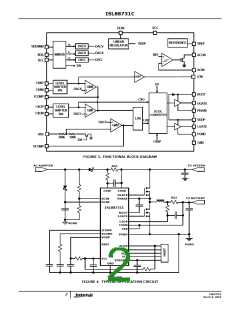
Functional Block Diagram .............................. 2
Typical Application Circuit ............................. 2
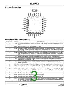
Pin Configuration ........................................... 3
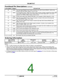
Functional Pin Descriptions ........................... 3
Ordering Information .................................... 4
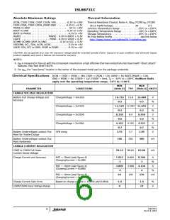
Absolute Maximum Ratings ........................... 6
Thermal Information ..................................... 6
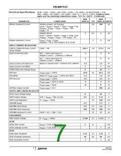
Electrical Specifications ................................. 6
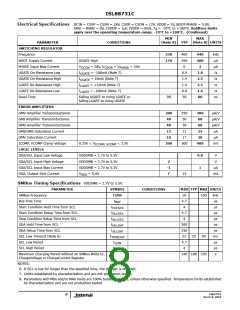
SMBus Timing Specifications ......................... 8
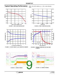
Typical Operating Performance ..........................9
Theory of Operation ....................................... 11
Inductor Selection ................................................17
Output Capacitor Selection .................................... 18
MOSFET Selection ................................................18
Snubber Design ...................................................19
Input Capacitor Selection ......................................19
Loop Compensation Design ................................... 19
Transconductance Amplifiers GMV, GMI and GMS ....19
PWM Gain Fm ...................................................... 19
Charge Current Control Loop .................................20
Adapter Current Limit Control Loop ........................20
Voltage Control Loop ............................................21
Output LC Filter Transfer Functions ........................21
Compensation Break Frequency Equations ..............22
Introduction ........................................................ 11
PWM Control ........................................................ 11
AC-Adapter Detection ........................................... 11
Current Measurement ........................................... 11
VDDP Regulator ................................................... 11
VDDSMB Supply .................................................. 11
Short Circuit Protection and 0V Battery Charging .... 11
Undervoltage Detect and Battery Trickle Charging ... 12
Over-Temperature Protection ................................ 12
The System Management Bus ............................... 12
General SMBus Architecture .................................. 12
Data Validity ........................................................ 12
START and STOP Conditions ............................... 12
Acknowledge ....................................................12
SMBus Transactions ..........................................12
PCB Layout Considerations .............................22
Power and Signal Layers Placement on the PCB ...... 22
Component Placement...........................................22
Signal Ground and Power Ground Connection ......... 23
GND and VCC Pin .................................................23
LGATE Pin ............................................................ 23
PGND Pin ............................................................. 23
PHASE Pin ...........................................................23
UGATE Pin ........................................................... 23
BOOT Pin ............................................................. 23
CSOP, CSON, CSSP and CSSN Pins ........................23
DCIN Pin .............................................................23
Copper Size for the Phase Node .............................23
Identify the Power and Signal Ground ....................23
Clamping Capacitor for Switching MOSFET ..............23
Byte Format ................................................... 13
ISL88731C and SMBus ................................... 13
Battery Charger Registers ............................. 13
Enabling and Disabling Charging ................... 13
Setting Charge Voltage .................................. 14
Setting Charge Current .................................. 15
Revision History ............................................. 24
Products ......................................................... 24
Package Outline Drawing ............................... 25
FN6978.0
March 8, 2010
5

 INTERSIL [ Intersil ]