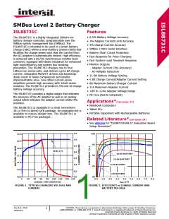
ISL88731C
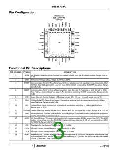
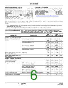
Pin Configuration
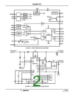
ISL88731C
(28 LD TQFN)
TOP VIEW
28 27 26 25 24 23 22
NC
ACIN
VREF
ICOMP
NC
VDDP
LGATE
PGND
CSOP
CSON
NC
1
2
3
4
5
6
7
21
20
19
18
17
16
15
PD
VCOMP
NC
VFB
8
9
10 11 12 13 14
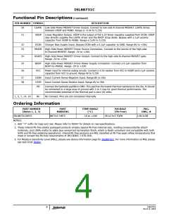
Functional Pin Descriptions
PIN NUMBER SYMBOL
DESCRIPTION
2
ACIN
AC Adapter Detection Input. Connect to a resistor divider from the AC adapter output. Range zero to
5.5V.
3
4
VREF
Reference Voltage output. Range 3.168V to 3.232V.
ICOMP Compensation Point for the charging current and adapter current regulation Loop. Connect 0.01µF
to GND. See “Voltage Control Loop” on page 21 for details on selecting the ICOMP capacitor. Range
zero to 5.5V.
6
VCOMP Compensation Point for the voltage regulation loop. Connect 4.7kΩ in series with 0.01µF to GND.
See “Voltage Control Loop” on page 21 for details on selecting VCOMP components. Range zero to
5.5V.
8
9
ICM
SDA
Input Current Monitor Output. ICM voltage equals 20 x (V
CSSP
- V ). Range zero to 3V.
CSSN
SMBus Data I/O. Open-drain Output. Connect an external pull-up resistor according to SMBus
specifications. Range zero to 5.5V.
10
SCL
SMBus Clock Input. Connect an external pull-up resistor according to SMBus specifications.
Range zero to 5.5V.
11
12
VDDSMB SMBus interface Supply Voltage Input. Bypass with a 0.1µF capacitor to GND. Range 3.3V to 5.5V.
GND
Analog Ground. Connect directly to the backside paddle. Connect to the backside paddle and PGND
at one point close to (under) the IC.
13
ACOK
AC Detect Output. This open drain output is high impedance when ACIN is greater than 3.2V. The ACOK
output remains low when the ISL88731C is powered down. Connect a 10k pull-up resistor from ACOK
to VDDSMB. Range 3.3V to 5.5V.
15
17
18
19
VFB
Feedback for the Battery Voltage. Range 1V to 19V.
Charge Current-Sense Negative Input. Range 1V to 19V.
Charge Current-Sense Positive Input. Range 1V to 19V.
CSON
CSOP
PGND
Power Ground. Connect PGND to the source of the low side MOSFET and the negative side of capacitors
to the charger output and the drain of the upper switching FET. Connect this area to the Backside paddle
at one location very near (under) the IC.
FN6978.0
March 8, 2010
3

 INTERSIL [ Intersil ]