ISL88731
takes control of the output (assuming that the adapter
60
40
20
0
current is below the limit set by ACLIM). The voltage error
amplifier (GMV) discharges the cap on VCOMP to limit the
output voltage. The current to the battery decreases as the
cells charge to the fixed voltage and the voltage across the
internal battery resistance decreases. As battery current
decreases the 2 current error amplifiers (GMI and GMS)
output their maximum current and charge the capacitor on
ICOMP to its maximum voltage (limited to 0.3V above
VCOMP). With high voltage on ICOMP, the minimum voltage
buffer output equals the voltage on VCOMP.
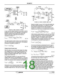
Compensator
Modulator
Loop
F
ZERO
-20
-40
-60
F
F
F
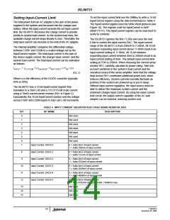
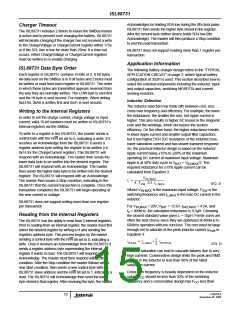
The voltage control loop is shown in Figure 23.
FILTER
POLE1
L
PHASE
POLE2
11
0.01
0.1
1
10
100
1000
RFET_RDSON
RL_DCR
FREQUENCY (kHz)
FIGURE 21. CHARGE CURRENT LOOP BODE PLOTS
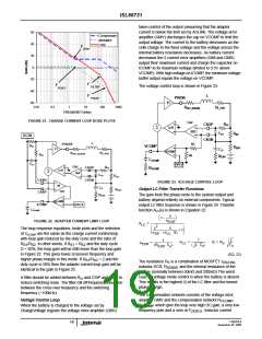
CA2
RF2
+
CSOP
CSON
Σ
0.25
+
S
20X
-
CF2
RS2
-
DCIN
L
R3
PHASE
RFET_RDSON
RS1
VCOMP
RBAT
-
GMV
+
11
CO
RL_DCR
RF1
R4
RESR
CVCOMP
RVCOMP
CF1
DACV
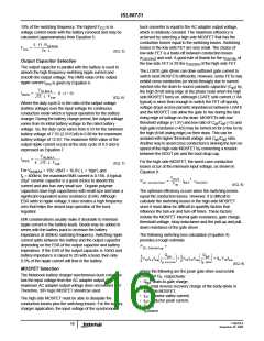
CA2
RF2
CSOP
CSON
+
0.25
+
S
Σ
20X
-
CF2
RS2
-
CSSN
CSSP
FIGURE 23. VOLTAGE CONTROL LOOP
-
+
20
CO
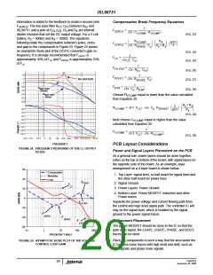
Output LC Filter Transfer Functions
The gain from the phase node to the system output and
RBAT
CA1
RESR
-
+
battery depend entirely on external components. Typical
output LC filter response is shown in Figure 24. Transfer
function ALC(s) is shown in Equation 22:
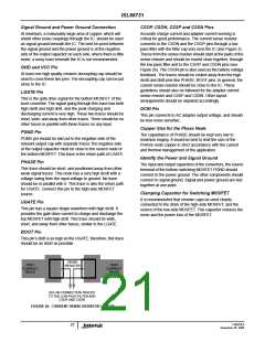
GMS
DACS
ICOMP
CICOMP
s
⎛
⎝
⎞
⎠
---------------
1 –
ω
FIGURE 22. ADAPTER CURRENT LIMIT LOOP
ESR
----------------------------------------------------------
A
=
LC
2
⎛
⎜
⎝
⎞
s
ω
s
The loop response equations, bode plots and the selection
of CICOMP are the same as the charge current control loop
with loop gain reduced by the duty cycle and the ratio of
----------- ------------------------
+
+ 1
⎟
(ω ⋅ Q)
LC
⎠
DP
1
L
C
o
1
-----------------------
ω
=
Q = R
⋅
------
--------------------------------
ω
=
LC
o
ESR
R
/R . In other words, if R = R and the duty cycle
(R
⋅ C )
( L ⋅ C )
S1 S2 S1 S2
ESR
o
o
D = 50%, the loop gain will be 6dB lower than the loop gain
in Figure 22. This gives lower crossover frequency and
(EQ. 22)
higher phase margin in this mode. If R /R = 2 and the
duty cycle is 50% then the adapter current loop gain will be
identical to the gain in Figure 22.
S1 S2
The resistance RO is a combination of MOSFET r
,
DS(ON)
inductor DCR, R
and the internal resistance of the
SENSE
battery (normally between 50mΩ and 200mΩ) The worst
case for voltage mode control is when the battery is absent.
This results in the highest Q of the LC filter and the lowest
phase margin.
A filter should be added between RS1 and CSIP and CSIN to
reduce switching noise. The filter roll off frequency should be
between the cross over frequency and the switching
frequency (~100kHz).
The compensation network consists of the voltage error
Voltage Control Loop
amplifier GMV and the compensation network R ,
VCOMP
C
which give the loop very high DC gain, a very low
When the battery is charged to the voltage set by
ChargeVoltage register the voltage error amplifier (GMV)
VCOMP
frequency pole and a zero at F
. Inductor current
ZERO1
FN9258.0
November 20, 2006
19

 INTERSIL [ Intersil ]