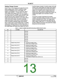
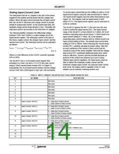
ISL88731
Low switching loss requires low drain-to-gate charge Q
.
Input Capacitor Selection
gd
Generally, the lower the drain-to-gate charge, the higher the
on-resistance. Therefore, there is a trade-off between the
on-resistance and drain-to-gate charge. Good MOSFET
selection is based on the Figure of Merit (FOM), which is a
product of the total gate charge and on-resistance. Usually,
the smaller the value of FOM, the higher the efficiency for
the same application.
The input capacitor absorbs the ripple current from the
synchronous buck converter, which is given by Equation 14:
V
(
V
−V
OUT
)
OUT IN
I
= I
BAT
rms
(EQ. 14)
V
IN
This RMS ripple current must be smaller than the rated RMS
current in the capacitor datasheet. Non-tantalum chemistries
(ceramic, aluminum, or OSCON) are preferred due to their
resistance to power-up surge currents when the AC adapter
is plugged into the battery charger. For Notebook battery
charger applications, it is recommended that ceramic
capacitors or polymer capacitors from Sanyo be used due to
their small size and reasonable cost.
For the low-side MOSFET, the worst-case power dissipation
occurs at minimum battery voltage and maximum input
voltage (Equation 10):
V
⎛
⎜
⎝
⎞
⎟
⎠
2
OUT
---------------
P
=
1 –
⋅ I
⋅ r
BAT DS(ON)
Q2
V
IN
(EQ. 10)
Choose a low-side MOSFET that has the lowest possible
on-resistance with a moderate-sized package like the SO-8
and is reasonably priced. The switching losses are not an
issue for the low-side MOSFET because it operates at
zero-voltage-switching.
Loop Compensation Design
ISL88731 has three closed loop control modes. One controls
the output voltage when the battery is fully charged or
absent. A second controls the current into the battery when
charging and the third limits current drawn from the adapter.
The charge current and input current control loops are
compensated by a single capacitor on the ICOMP pin. The
voltage control loop is compensated by a network on the
VCOMP pin. Descriptions of these control loops and
guidelines for selecting compensation components will be
given in the following sections. Which loop controls the
output is determined by the minimum current buffer and the
minimum voltage buffer shown in the Block Diagram. These
three loops will be described separately.
Ensure that the required total gate drive current for the
selected MOSFETs should be less than 24mA. So, the total
gate charge for the high-side and low-side MOSFETs is
limited by Equation 11:
I
GATE
----------------
Q
≤
GATE
f
(EQ. 11)
sw
Where I
GATE
is the total gate drive current and should be
less than 24mA. Substituting I
= 24mA and f = 400kHz
GATE
s
into the above equation yields that the total gate charge
should be less than 80nC. Therefore, the ISL88731 easily
drives the battery charge current up to 8A.
Transconductance Amplifiers GMV, GMI and GMS
ISL88731 uses several transconductance amplifiers (also
known as gm amps). Most commercially available op amps
are voltage controlled voltage sources with gain expressed
Snubber Design
ISL88731's buck regulator operates in discontinuous current
mode (DCM) when the load current is less than half the
peak-to-peak current in the inductor. After the low-side FET
turns off, the phase voltage rings due to the high impedance
with both FETs off. This can be seen in Figure 9. Adding a
snubber (resistor in series with a capacitor) from the phase
node to ground can greatly reduce the ringing. In some
situations a snubber can improve output ripple and
regulation.
as A = V
/V . gm amps are voltage controlled current
sources with gain expressed as gm = I /V . gm will
OUT IN
OUT IN
appear in some of the equations for poles and zeros in the
compensation.
PWM Gain F
m
The Pulse Width Modulator in the ISL88731 converts voltage
at VCOMP to a duty cycle by comparing VCOMP to a
triangle wave (duty = VCOMP/V
). The low-pass
filter formed by L and C convert the duty cycle to a DC
PP RAMP
The snubber capacitor should be approximately twice the
parasitic capacitance on the phase node. This can be
estimated by operating at very low load current (100mA) and
measuring the ringing frequency.
O
output voltage (Vo = V
*duty). In ISL88731, the triangle
DCIN
wave amplitude is proportional to V . Making the ramp
DCIN
amplitude proportional to DCIN makes the gain from
VCOMP to the PHASE output a constant 11 and is
independent of DCIN. For small signal AC analysis, the
battery is modeled by its internal resistance. The total output
resistance is the sum of the sense resistor and the internal
resistance of the MOSFETs, inductor and capacitor.
Figure19 shows the small signal model of the pulse width
modulator (PWM), power stage, output filter and battery.
C
and R
can be calculated from Equations 12
SNUB
SNUB
and 13:
2
2 ⋅ L
------------------------------------
C
=
R
=
-------------------
SNUB
2
SNUB
C
(2πF
)
⋅ L
SNUB
ring
(EQ. 13)
(EQ. 12)
FN9258.0
November 20, 2006
17

 INTERSIL [ Intersil ]