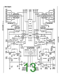
ISL6227
PG2/REF (Pin 16)
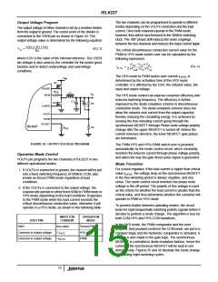
This pin has a double function, depending on the mode of
operation.
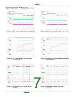
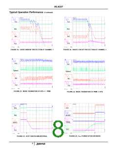
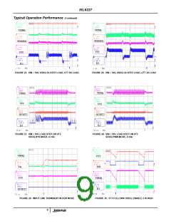
Typical Application
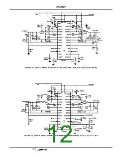
Figures 31 and 32 show the application circuits of a dual
channel DC/DC converter for a notebook PC.
When the chip is used as a dual channel PWM controller
(DDR = 0), the pin provides an open drain PGOOD2 function
for the second channel the same way as PG1. The pin is
pulled low when the second channel output is out of
-11% -- +15% of the set value.
The power supply in Figure 31 provides +2.5V and +1.8V
voltages for memory and the graphics interface chipset from
a +5.0-24VDC battery voltage.
Figure 32 illustrates the application circuit for a DDR memory
power solution. The power supply shown in Figure 32
generates +2.5V VDDQ voltage from a battery. The +1.25V
VTT termination voltage tracks VDDQ/2 and is derived from
+2.5V VDDQ. To complete the DDR memory power
requirements, the +1.25V reference voltage is provided
through the PG2 pin.
In DDR mode (DDR=1), this pin is the output of the buffer
amplifier that takes VDDQ/2 voltage applied to OCSET2 pin
from the resister divider. It can source a typical 10mA
current.
OCSET2 (Pin 18)
In a dual channel application with DDR = 0, a resistor from
this pin to ground sets the overcurrent threshold for the
second channel controller. Its voltage is the buffered internal
0.9V reference.
In the DDR application with DDR=1, this pin connects to the
center point of a resistor divider tracking the VDDQ/2. This
voltage is then buffered by an amplifier voltage follower and
sent to the PG2/REF pin. It sets the reference voltage of
channel 2 for its regulation.
VCC (Pin 28)
This pin powers the controller.
11

 INTERSIL [ Intersil ]