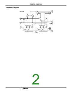
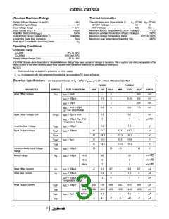
CA3280, CA3280A
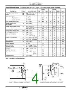
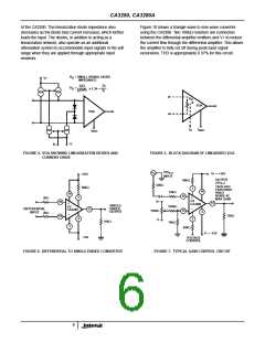
of the CA3280. The linearization diode impedance also
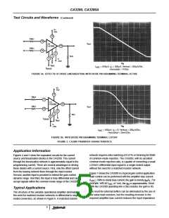
Figure 10 shows a triangle wave to sine wave converter
using the CA3280. Two 100kΩ resistors are connected
between the differential amplifier emitters and V+ to reduce
the current flow through the differential amplifier. This allows
the amplifier to fully cut off during peak input signal
excursions. THD is appropriately 0.37% for this circuit.
decreases as the diode bias current increases, which further
loads the input. The diodes, in addition to acting as a
linearization network, also operate as an additional
attenuation system to accommodate input signals in the volt
range when they are applied through appropriate input
resistors.
R
R
= SMALL SIGNAL DIODE
IMPEDANCE
D
V+
52Ω
70
≈
D
x 1.34 =
I (mA)
I
D
D
R
D
VOA
VOA
I
ABC
I
D
I
ABC
I
V-
D
FIGURE 4. VOA SHOWING LINEARIZATION DIODES AND
CURRENT DRIVE
FIGURE 5. BLOCK DIAGRAM OF LINEARIZED VOA
10V
P-P
INPUT
V+ = +15V
OUTPUT
+15V
68kΩ
21V
P-P
600Ω
14mV AGC
FEEDTHRU
400µV
68kΩ
1
14
10kΩ
14
NOISE AT
MAX GAIN
16
3
+
1/2
CA3280
2kΩ
V+
16
+
13
SINGLE-
330kΩ
10kΩ
1/2
CA3280
ENDED
-
DIFFERENTIAL
INPUT
13
15
100kΩ
V-
4
OUTPUT
2kΩ
-
15kΩ
15
4
3
10kΩ
1
20kΩ
V- = -15V
-15V
VOLTAGE
CONTROL
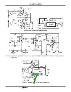
FIGURE 6. DIFFERENTIAL TO SINGLE ENDED CONVERTER
FIGURE 7. TYPICAL GAIN CONTROL CIRCUIT
6

 INTERSIL [ Intersil ]