CA3280, CA3280A
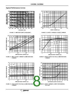
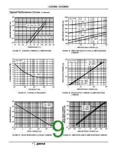
Typical Performance Curves (Continued)
4
4
10
10
V
= ±15V
S
V
= ±15V
S
3
2
10
10
3
10
2
10
o
o
T
A
= 125 C
T
= 125 C
A
1
10
o
T
= 25 C
A
o
o
T
= -55 C, 25 C
1
A
10
1
o
T
= -55 C
A
-1
10
1
10
-1
1
2
3
-1
1
2
3
1
10
10
10
10
1
10
10
10
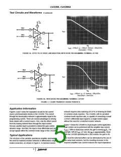
AMPLIFIER BIAS CURRENT (µA)
AMPLIFIER BIAS CURRENT (µA)
FIGURE 23. SUPPLY CURRENT vs AMPLIFIER BIAS CURRENT
FIGURE 24. INPUT BIAS CURRENT vs AMPLIFIER BIAS
CURRENT
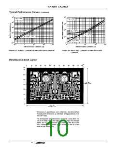
Metallization Mask Layout
Dimensions in parentheses are in millimeters and derived from
the basic inch dimensions as indicated. Grid graduations are in
-3
mils (10 inch).
The photographs and dimensions represent a chip when it is
part of the wafer. When the wafer is cut into chips, the cleavage
o
o
angles are 57 instead of 90 with respect to the face of the
chip. Therefore, the isolated chip is actually 7 mils (0.17mm)
larger in both dimensions.
10

 INTERSIL [ Intersil ]