CA3280, CA3280A
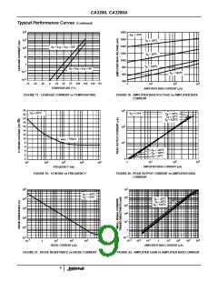
Test Circuits and Waveforms (Continued)
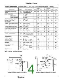
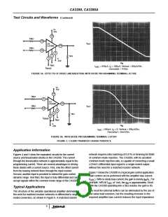
V+
15V
14
10kΩ
10kΩ
16
15
I
OUT
1/2
CA3280
13
4
3
1
1kΩ
V-
-15V
V
IN
I
ABC
I
= 650µA, I = 200µA; Vertical = 200µA/Div.;
ABC
D
I
DIODE
Horizontal = 1V/Div.
FIGURE 3A. EFFECTS OF DIODE LINEARIZATION, WITH DIODE PROGRAMMING TERMINAL ACTIVE
V+
15V
11
10kΩ
9
1/2
CA3280
12
I
10kΩ
OUT
10
6
4
8
1kΩ
I
DIODE
I
ABC
V-
-15V
V
IN
I
= 650µA; I = 0; Vertical = 200µA/Div.;
ABC
D
Horizontal = 25mV/Div.
FIGURE 3B. WITH DIODE PROGRAMMING TERMINAL CUTOFF
FIGURE 3. CA3280 TRANSFER CHARACTERISTICS
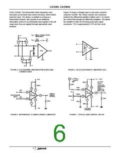
Application Information
Figures 4 and 5 show the equivalent circuits for the current
source and linearization diodes in the CA3280. The current
through the linearization network is approximately equal to the
programming current. There are several advantages to driving
these diodes with a current source. First, only the offset current
from the biasing network flows through the input resistor.
Second, another input is provided to extend the gain control
dynamic range. And third, the input is truly differential and can
accept signals within the common mode range of the CA3280.
network requires ratio matching of 0.01% or trimming for 80dB
of common-mode rejection. The CA3280, with its excellent
common mode rejection ratio, is capable of converting a small
(±25mV) differential input signal to a single-ended output
without the need for a matched resistor network.
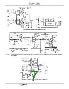
Figure 7 shows the CA3280 in a typical gain control application.
Gain control can be performed with the amplifier bias current
(l
). With no diode bias current, the gain is merely g R . For
ABC
M L
example, with an l
ABC
of 1mA, the g is approximately 16mS.
M
With the CA3280 operating into a 5kΩ resistor, the gain is 80.
Typical Applications
The need for external buffers can be eliminated by the use of
low value load resistors, but the resulting increase in the
required amplifier bias current reduces the input impedance
The structure of the variable operational amplifier eliminates
the need for matched resistor networks in differential to single
ended converters, as shown in Figure 6. A matched resistor
5

 INTERSIL [ Intersil ]