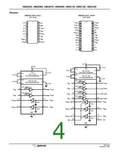
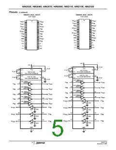
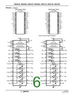
HIN202E, HIN206E, HIN207E, HIN208E, HIN211E, HIN213E, HIN232E
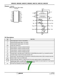
Pinouts (Continued)
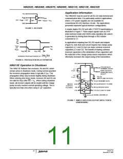
HIN232E (PDIP, SOIC, SSOP, TSSOP)
TOP VIEW
+5V
16
V
1
2
3
4
5
6
7
8
16
15
14
13
12
1
CC
C1+
V+
V
CC
0.1µF
C1+
+
+
+
+
2
+5V TO 10V
VOLTAGE INVERTER
0.1µF
0.1µF
GND
T1
V+
V-
3
4
C1-
C1-
C2+
C2-
V-
OUT
C2+
R1
R1
T1
IN
+10V TO -10V
VOLTAGE INVERTER
6
5
C2-
0.1µF
OUT
11
10
9
IN
IN
+5V
T1
14
400kΩ
11
T2
T2
R2
OUT
T1
T1
IN
OUT
R2
IN
OUT
+5V
T2
400kΩ
10
12
7
T2
R1
T2
IN
OUT
13
R1
IN
OUT
OUT
5kΩ
5kΩ
R1
9
8
R2
R2
IN
R2
GND
15
Pin Des criptions
PIN
FUNCTION
V
Power Supply Input 5V ±10%, (5V ±5% HIN207E).
Internally generated positive supply (+10V nominal).
Internally generated negative supply (-10V nominal).
Ground Lead. Connect to 0V.
CC
V+
V-
GND
C1+
C1-
External capacitor (+ terminal) is connected to this lead.
External capacitor (- terminal) is connected to this lead.
External capacitor (+ terminal) is connected to this lead.
External capacitor (- terminal) is connected to this lead.
C2+
C2-
T
Transmitter Inputs. These leads accept TTL/CMOS levels. An internal 400kΩ pull-up resistor to V is connected to each lead.
IN
CC
T
Transmitter Outputs. These are RS-232 levels (nominally ±10V).
OUT
R
Receiver Inputs. These inputs accept RS-232 input levels. An internal 5kΩ pull-down resistor to GND is connected to each input.
Receiver Outputs. These are TTL/CMOS levels.
IN
R
OUT
EN, EN
SD, SD
Receiver Enable Input. With EN = 5V (HIN213E EN=0V), the receiver outputs are placed in a high impedance state.
Shutdown Input. With SD = 5V (HIN213E SD = 0V), the charge pump is disabled, the receiver outputs are in a high impedance
state (except R4 and R5 of HIN213E) and the transmitters are shut off.
NC
No Connect. No connections are made to these leads.
FN4315.16
7
November 4, 2005

 INTERSIL [ Intersil ]