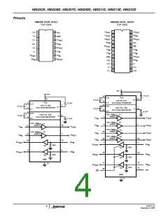
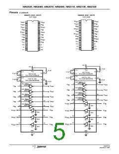
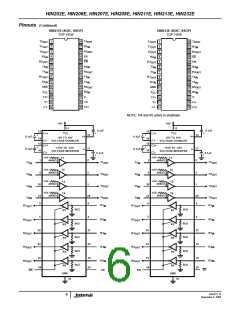
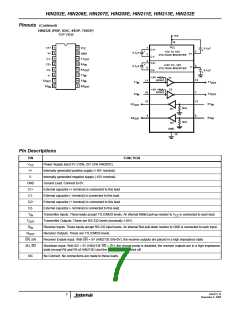
HIN202E, HIN206E, HIN207E, HIN208E, HIN211E, HIN213E, HIN232E
Absolute Maximum Ratings
Thermal Information
V
to Ground. . . . . . . . . . . . . . . . . . . . . . (GND -0.3V) < V
< 6V
-0.3V) < V+ < 12V
Thermal Resistance (Typical, Note 1)
θJA (°C/W)
CC
V+ to Ground . . . . . . . . . . . . . . . . . . . . . . . .(V
CC
CC
16 Ld SOIC (N) Package . . . . . . . . . . . . . . . . . . . . .
16 Ld SOIC (W) Package. . . . . . . . . . . . . . . . . . . . .
16 Ld SSOP Package . . . . . . . . . . . . . . . . . . . . . . .
16 Ld TSSOP Package . . . . . . . . . . . . . . . . . . . . . .
16 Ld PDIP Package* . . . . . . . . . . . . . . . . . . . . . . .
24 Ld SOIC Package . . . . . . . . . . . . . . . . . . . . . . . .
24 Ld SSOP Package . . . . . . . . . . . . . . . . . . . . . . .
28 Ld SOIC Package . . . . . . . . . . . . . . . . . . . . . . . .
28 Ld SSOP Package . . . . . . . . . . . . . . . . . . . . . . .
Maximum Junction Temperature (Plastic Package) . . . . . . . . 150°C
Maximum Storage Temperature Range . . . . . . . . . .-65°C to 150°C
Maximum Lead Temperature (Soldering 10s) . . . . . . . . . . . . . 300°C
(SOIC and SSOP - Lead Tips Only)
110
100
155
145
90
75
135
70
V- to Ground . . . . . . . . . . . . . . . . . . . . . . .-12V < V- < (GND +0.3V)
Input Voltages
T
R
. . . . . . . . . . . . . . . . . . . . . . . . . . . . . -0.3V < V < (V+ +0.3V)
IN
IN
. . . . . . . . . . . . . . . . . . . . . . . . . . . . . . . . . . . . . . . . . . . . ±30V
IN
Output Voltages
T
R
. . . . . . . . . . . . . . . . . . . .(V- -0.3V) < V
. . . . . . . . . . . . . . . . . (GND -0.3V) < V
< (V+ +0.3V)
< (V+ +0.3V)
OUT
TXOUT
RXOUT
OUT
Short Circuit Duration
100
T
R
. . . . . . . . . . . . . . . . . . . . . . . . . . . . . . . . . . . . . .Continuous
. . . . . . . . . . . . . . . . . . . . . . . . . . . . . . . . . . . . . .Continuous
OUT
OUT
ESD Classification . . . . . . . . . . . . . . . . . . . . See Specification Table
Operating Conditions
*Pb-free PDIPs can be used for through hole wave solder
processing only. They are not intended for use in Reflow solder
processing applications.
Temperature Range
HIN2XXECX. . . . . . . . . . . . . . . . . . . . . . . . . . . . . . . . 0°C to 70°C
HIN2XXEIX. . . . . . . . . . . . . . . . . . . . . . . . . . . . . . . .-40°C to 85°C
CAUTION: Stresses above those listed in “Absolute Maximum Ratings” may cause permanent damage to the device. This is a stress only rating and operation of the
device at these or any other conditions above those indicated in the operational sections of this specification is not implied.
NOTE:
1. θ is measured with the component mounted on an evaluation PC board in free air.
JA
Electrical Specifications Test Conditions: V = +5V ±10%, (V = +5V ±5% HIN207E); C1-C4 = 0.1µF; T = Operating Temperature
CC
CC
A
Range
PARAMETER
SUPPLY CURRENTS
Power Supply Current, I
TEST CONDITIONS
MIN
TYP
MAX
UNITS
No Load,
HIN202E
-
-
8
15
20
mA
mA
CC
T
= 25°C
A
HIN206E - HIN208E, HIN211E,
HIN213E
11
HIN232E
-
-
-
5
1
10
10
50
mA
µA
µA
Shutdown Supply Current, I (SD)
CC
T
= 25°C
HIN206E, HIN211E
HIN213E
A
15
LOGIC AND TRANSMITTER INPUTS, RECEIVER OUTPUTS
Input Logic Low, V
T
T
, EN, SD, EN, SD
-
2.0
2.4
-
-
0.8
-
V
V
lL
IN
Input Logic High, V
-
lH
IN
EN, SD, EN, SD
= 0V
-
-
V
Transmitter Input Pullup Current, I
T
15
0.1
4.6
0.5
200
0.4
-
µA
V
P
IN
TTL/CMOS Receiver Output Voltage Low, V
I
I
= 1.6mA (HIN202E, HIN232E, I
= 3.2mA)
OUT
-
OL
OUT
OUT
TTL/CMOS Receiver Output Voltage High, V
TTL/CMOS Receiver Output Leakage
RECEIVER INPUTS
= -1mA
3.5
-
V
OH
EN = V , EN = 0, 0V < R
CC OUT
< V
±10
µA
CC
RS-232 Input Voltage Range, V
-30
-
+30
7.0
-
V
kΩ
V
IN
Receiver Input Impedance, R
T
= 25°C, V = ±3V
3.0
5.0
1.2
1.5
1.7
1.5
0.5
IN
A IN
Receiver Input Low Threshold, V (H-L)
V
= 5V,
Active Mode
-
IN
CC
= 25°C
T
A
Shutdown Mode HIN213E R4 and R5
Active Mode
-
-
-
V
Receiver Input High Threshold, V (L-H)
IN
V
= 5V,
2.4
2.4
1.0
V
CC
= 25°C
T
A
Shutdown Mode HIN213E R4 and R5
-
V
Receiver Input Hysteresis, V
V
= 5V, No Hysteresis in Shutdown Mode
CC
0.2
V
HYST
FN4315.16
8
November 4, 2005

 INTERSIL [ Intersil ]