E
28F020
NOTES:
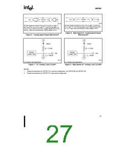
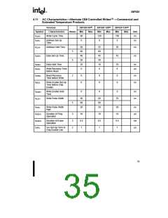
1. Read timing characteristics during read/write operations are the same as during read-only operations. Refer to AC
Characteristics for Read-Only Operations.
2. Guaranteed by design.
3. The integrated stop timer terminates the programming/erase operations, thus eliminating the need for a maximum
specification.
4. See High Speed AC Testing Input/Output Waveform (Figure 8) and High Speed AC Testing Load Circuit (Figure 9) for
testing characteristics.
5. Minimum Specification for Extended Temperature product.
6. See Testing Input/Output Waveform (Figure 6) and AC Testing Load Circuit (Figure 7) for testing characteristics.
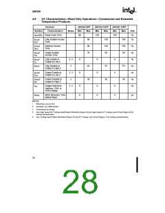
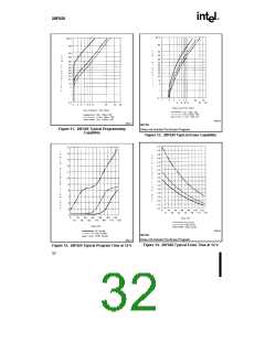
4.10
Erase and Programming Performance
Limits
Parameter
Notes
1, 3, 4
1, 2, 4
Min
Typ
2
Max
30
Unit
Sec
Sec
Chip-Erase Time
Chip-Program Time
4
25
NOTES:
1. “Typicals” are not guaranteed, but based on a limited number of samples from production lots. Data taken at 25 °C, 12.0 V
PP at 0 cycles.
V
2. Minimum byte programming time excluding system overhead is 16 µsec (10 µsec program + 6 µsec write recovery), while
maximum is 400 µsec/byte (16 µsec x 25 loops allowed by algorithm). Max chip-programming time is specified lower than
the worst case allowed by the programming algorithm since most bytes program significantly faster than the worst case
byte.
3. Excludes 00H programming prior to erasure.
4. Excludes System-Level Overhead.
31

 INTEL [ INTEL ]