Page 10
Electrical Characteristics
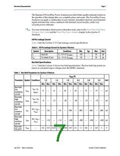
Table 10 lists the OCT variation with temperature and voltage after the power-up
calibration. The OCT variation is valid for a VCCIO range of 5% and a temperature
range of 0° to 85°C.
Table 10. OCT Variation after Power-Up Calibration for Cyclone V Devices
Symbol
Description
VCCIO (V)
3.0
Typical
0.100
0.100
0.100
0.100
0.150
0.150
0.150
0.189
0.208
0.266
0.273
0.200
0.200
0.317
Unit
2.5
1.8
OCT variation with voltage without
recalibration
dR/dV
1.5
%/mV
1.35
1.25
1.2
3.0
2.5
1.8
OCT variation with temperature
without recalibration
dR/dT
1.5
%/°C
1.35
1.25
1.2
Pin Capacitance
Table 11 lists the Cyclone V device family pin capacitance.
Table 11. Pin Capacitance for Cyclone V Devices
Symbol
CIOTB
Description
Value
Unit
pF
Input capacitance on top and bottom I/O pins
Input capacitance on left and right I/O pins
6
6
6
CIOLR
pF
COUTFB
Input capacitance on dual-purpose clock output and feedback pins
pF
Hot Socketing
Table 12 lists the hot socketing specifications for Cyclone V devices.
Table 12. Hot Socketing Specifications for Cyclone V Devices
Symbol
IIOPIN (DC)
Description
DC current per I/O pin
Maximum
300 μA
(1)
IIOPIN (AC)
AC current per I/O pin
8 mA
IXCVR-TX (DC)
IXCVR-RX (DC)
Note to Table 12:
DC current per transceiver transmitter (TX) pin
DC current per transceiver receiver (RX) pin
100 mA
50 mA
(1) The I/O ramp rate is 10 ns or more. For ramp rates faster than 10 ns, |IIOPIN| = C dv/dt, in which C is the I/O pin
capacitance and dv/dt is the slew rate.
Cyclone V Device Datasheet
July 2014 Altera Corporation

 INTEL [ INTEL ]