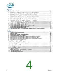
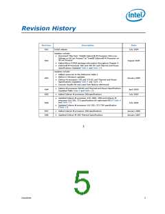
Contents
1
Introduction..............................................................................................................7
1.1
1.2
Terminology .......................................................................................................8
References .........................................................................................................8
2
Low Power Features................................................................................................ 11
2.1
Clock Control and Low Power States .................................................................... 11
2.1.1 Normal State......................................................................................... 11
2.1.2 AutoHALT Power-Down State ................................................................... 11
2.1.3 Stop-Grant State.................................................................................... 11
2.1.4 HALT/Grant Snoop State ......................................................................... 12
2.1.5 Sleep State ........................................................................................... 12
2.1.6 Deep Sleep State ................................................................................... 13
FSB Low Power Enhancements............................................................................ 13
Processor Power Status Indicator (PSI#) Signal..................................................... 14
2.2
2.3
3
Electrical Specifications........................................................................................... 15
3.1
Power and Ground Pins ...................................................................................... 15
3.1.1 FSB Clock (BCLK[1:0]) and Processor Clocking........................................... 15
Voltage Identification and Power Sequencing ........................................................ 15
Catastrophic Thermal Protection.......................................................................... 17
Signal Terminations and Unused Pins................................................................... 17
FSB Frequency Select Signals (BSEL[1:0])............................................................ 17
FSB Signal Groups............................................................................................. 17
CMOS Signals ................................................................................................... 19
Maximum Ratings.............................................................................................. 19
Processor DC Specifications ................................................................................ 19
3.2
3.3
3.4
3.5
3.6
3.7
3.8
3.9
4
5
Package Mechanical Specifications and Pin Information.......................................... 29
4.1
4.2
Processor Pinout and Pin List .............................................................................. 37
Alphabetical Signals Reference............................................................................ 55
Thermal Specifications and Design Considerations .................................................. 63
5.1
Thermal Specifications ....................................................................................... 65
5.1.1 Thermal Diode ....................................................................................... 65
5.1.2 Thermal Diode Offset.............................................................................. 66
5.1.3 Intel® Thermal Monitor........................................................................... 67
Datasheet
3

 INTEL [ INTEL ]