Electrical Characteristics
11.3
Buffer Supply and DC Characteristics
11.3.1
I/O Buffer Supply Voltages
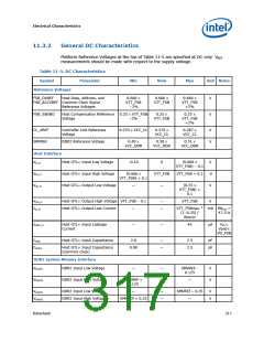
The I/O buffer supply voltage is measured at the GMCH package pins. The tolerances
shown in Table 11-4 are inclusive of all noise from DC up to 20 MHz. In the lab, the
voltage rails should be measured with a bandwidth limited oscilloscope with a roll off
of 3 dB/decade above 20 MHz under all operating conditions.
Table 11-4 indicates which supplies are connected directly to a voltage regulator or to
a filtered voltage rail. For voltages that are connected to a filter, they should me
measured at the input of the filter.
If the recommended platform decoupling guidelines cannot be met, the system
designer will have to make tradeoffs between the voltage regulator output DC
tolerance and the decoupling performance of the capacitor network to stay within the
voltage tolerances listed in Table 11-4.
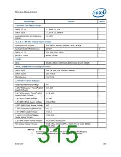
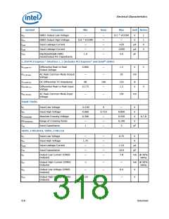
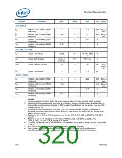
Table 11-4. I/O Buffer Supply Voltage
Symbol
VCCSM
Parameter
DDR2 I/O Supply Voltage
Min
Nom
Max
Unit Notes
1.7
1.7
1.8
1.8
1.25
3.3
1.2
1.1
1.9
1.9
V
V
V
V
V
V
5
2
VCC_SMCLK
VCC_EXP
DDR2 Clock Supply Voltage
SDVO, PCI Express* Supply Voltage
SDVO, PCI Express* Analog Supply Voltage
1.2 V System Bus Input Supply Voltage
1.1 V System Bus Input Supply Voltage
1.188
3.135
1.14
1.045
1.313
3.465
1.26
1.155
VCCA_EXP
2
4
VTT
VCC
MCH Core Supply Voltage
1.188
1.25
1.313
V
VCC_CL
Controller Supply Voltage
1.188
3.135
3.135
1.425
1.425
1.188
1.25
3.3
1.313
3.465
3.465
1.575
1.575
1.313
V
V
V
V
V
V
VCC3_3
CMOS Supply Voltage
VCCA_DAC
VCCD_CRT
VCCDQ_CRT
Display DAC Analog Supply Voltage
Display Digital Supply Voltage
Display Quiet Digital Supply Voltage
Various PLLs’ Analog Supply Voltages
3.3
3
1
1.5
1.5
1
VCCA_HPLL,
VCCA_EXPPLL,
VCCA_DPLLA,
VCCA_DPLLB,
VCCA_MPLL
1.25
2,7
NOTES:
1. The VCCD_CRT and VCCDQ_CRT can also operate at a nominal 1.8 V ±5% input voltage. Only
the 1.5 V nominal voltage setting will be validated internally.
2. These rails are filtered from other voltage rails on the platform and should be measured at the
input of the filter.
3. VCCA_DAC voltage tolerance should only be measured when the DAC is turned ON and at a
stable resolution setting. Any noise on the DAC during power on or display resolution changes do
not impact the circuit.
4. GMCH supports both VTT = 1.2 V nominal and VTT = 1.1 V nominal depending on the identified
processor.
316
Datasheet

 INTEL [ INTEL ]