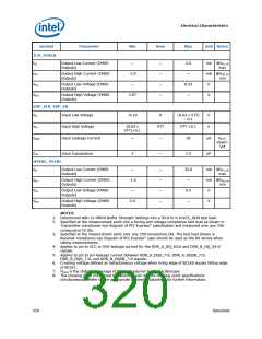
Electrical Characteristics
Symbol
Parameter
Min
Nom
Max
Unit Notes
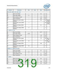
ICH_SYNCB
IOL
Output Low Current (CMOS
Outputs)
—
-2.0
—
—
—
—
—
2.0
—
mA @VOL_HI
max
IOH
VOL
VOH
Output High Current (CMOS
Outputs)
mA @VOH_HI
min
Output Low Voltage (CMOS
Outputs)
0.33
—
V
Output High Voltage (CMOS
Outputs)
2.97
V
EXP_SLR, EXP_EN
VIL
Input Low Voltage
-0.10
0
VTT
—
(0.63 x VTT)
– 0.1
V
V
VIH
Input High Voltage
(0.63 x
VTT)+0.1
VTT +0.1
ILEAK
Input Leakage Current
—
20
μA
VOL<
Vpad<
Vtt
CIN
Input Capacitance
2
—
2.5
pF
HSYNC, VSYNC
IOL
Output Low Current (CMOS
Outputs)
—
-1.0
—
—
—
—
—
35.0
—
mA @VOL_HI
max
IOH
VOL
VOH
Output High Current (CMOS
Outputs)
mA @VOH_HI
min
Output Low Voltage (CMOS
Outputs)
0.5
—
V
Output High Voltage (CMOS
Outputs)
2.4
V
NOTES:
1. Determined with 2x GMCH Buffer Strength Settings into a 50 Ω to 0.5xVCC_DDR test load.
2. Specified at the measurement point into a timing and voltage compliance test load as shown in
Transmitter compliance eye diagram of PCI Express* specification and measured over any 250
consecutive TX Uls.
3. Specified at the measurement point over any 250 consecutive Uls. The test load shown in
Receiver compliance eye diagram of PCI Express* spec should be used as the RX device when
taking measurements.
4. Applies to pin to VCC or VSS leakage current for the DDR_A_DQ_63:0 and DDR_B_DQ_63:0
signals.
5. Applies to pin to pin leakage current between DDR_A_DQS_7:0, DDR_A_DQSB_7:0,
DDR_B_DQS_7:0, and DDR_B_DQSB_7:0 signals.
6. Crossing voltage defined as instantaneous voltage when rising edge of BCLK0 equals falling edge
of BCLK1.
7. VHavg is the statistical average of the VH measured by the oscilloscope.
8. The crossing point must meet the absolute and relative crossing point specifications
simultaneously. Refer to the appropriate processor datasheet for further information.
320
Datasheet

 INTEL [ INTEL ]