IA186ES/IA188ES
Data Sheet
8-Bit/16-Bit Microcontrollers
November 15, 2011
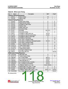
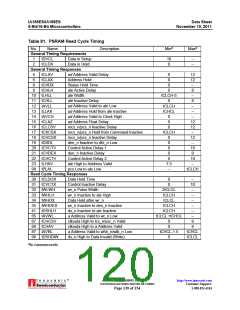
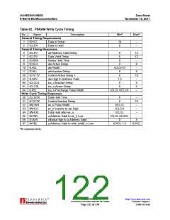
Table 82. PSRAM Write Cycle Timing
a
a
No.
Name
Description
Min
Max
General Timing Requirements
1
2
tDVCL
tCLDX
Data in Setup
Data in Hold
10
0
–
–
General Timing Responses
5
7
8
9
tCLAV
tCLDV
tCHDX
tCHLH
ad Address Valid Delay
Data Valid Delay
Status Hold Time
ale Active Delay
0
0
0
0
12
12
–
8
10 tLHLL
11 tCHLL
20 tCVCTV
23 tLHAV
80 tCLCLX
81 tCLCSL
84 tLRLL
ale Width
tCLCH-5
–
8
10
–
9
ale Inactive Delay
Control Active Delay 1
ale High to Address Valid
lcs_n Inactive Delay
lcs_n Active Delay
lcs_n Precharge Pulse Width
0
0
7.5
0
0
9
–
tCLCL+tCLCH
Write Cycle Timing Responses
30 tCLDOX
31 tCVCTX
32 tWLWH
33 tWHLH
34 tWHDX
65 tAVWL
68 tCHAV
87 tAVBL
Data Hold Time
Control Inactive Delay
wr_n Pulse Width
wr_n Inactive to ale High
Data Hold after wr_n
a Address Valid to wr_n Low
clkouta High to a Address Valid
a Address Valid to whb_n/wlb_n Low
0
0
–
10
–
–
–
–
8
2tCLCL
tCLCH
tCLCL
tCLCL+tCHCL
0
tCHCL-1.5
tCHCL
a
In nanoseconds.
®
IA211050902-19
UNCONTROLLED WHEN PRINTED OR COPIED
http://www.innovasic.com
Customer Support:
Page 122 of 154
1-888-824-4184

 INNOVASIC [ INNOVASIC, INC ]